Facebook
 Google
 GitHub
 Linkedin
High Power Digital Inrush Current Controller
This article highlights IXYS HPDICC that offers flexibility in implementing a unique control algorithm for the development of an efficient power system.
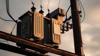
Inrush current creates limitations in power supplies and affects reliability due to overstress caused by the huge surge in initial current at power-up. Known solutions to limit inrush current [1], [2] require resistors or conventional NTC thermistors which cause significant power loss and decrease efficiency.
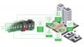
Our approach [3] illustrates the advantages of digital power control that overcome many of the disadvantages of the existing technology and boosts interest in the digital control of high power converters, thereby stimulating the development of the next generation of these devices. IXYS’ High Power Digital Inrush Current Controller (HPDICC), which is the second step in developing this new approach, is tested for load currents up to 10A. Industrial AC-DC, DC-AC power supplies such as battery chargers, motor drives, and solar inverters with rat-ings ≤5 kW can implement this design to control large inrush current.
IXYS High Power Digital Inrush Current Control technology extends to high current levels while also introducing high current Power MOSFET (MMIX1T132N50P3) with monolithically integrated current sense mirror and two temperature sense diodes. This design utilizes Zilog’s 8-bit Z8F3281 MCU and other IXYS components such as a rectifier and driver ICs.
Key Advantages
The High Power Digital Inrush Current Controller offers the following advantages:
- High-efficiency solution with a few components that can be reused for other goals after pre-charge is complete; for example, in PFC/boost converters, where the same inductor, output capacitors, and MCU will be utilized.
- Scalable design that can be adjusted to the desired inrush current by replacing a few critical components and making minor software corrections.
- Easy-to- replicate design that does not require any adjustment from one sample to another to obtain the expected result and maximum efficiency.
This inrush controller is tested for a load current up to 10A. The load current may be substantially increased since the power MOSFET used in the design is rated at 120A and a serial current sense resistor for a main current is not present. In order to increase the load current beyond 10A, the designer is required to change the current mirror sensor resistor, a bridge rectifier, and an inductor to be compatible with the increased current rating.
Figure 1 illustrates a circuit schematic in which the key idea is to provide charge to the bulk capacitor in equal increments. The Capacitor (C) is charged by a power MOSFET (SW1) driven according to a time-dependent pulse train. The pulse sequence is designed to provide equal voltage increments at the capacitor and maintains a peak of charging current at about the same value at each cycle. The number of cycles depends on the capacitor’s value, which is selected based on the desired amplitude of the ripple voltage at the output. The charge current is a function of the number of pulses and the timing position with respect to the rectified sine wave.
Figure 2 shows a typical pulse train for SW1. If we consider N cycles for inrush control, then we can split the normalized amplitude of the half-rectified sine wave into N segments with 1/N increment. During Cycle 1, SW1 is ON (conducting) from the time stamp t1 to T, allowing the capacitor C charge to the voltage proportional to normalized value 1/N. The charging current does not rise instantly, because it is a current in serial LC resonant circuit. That shapes the current waveform to the resonant one. The current is rising until the capacitor voltage reaches the input voltage.

Figure 1: Circuit Schematic for Digital Inrush Controller

Figure 2: Digital Inrush Control Timing
The current then continues its resonant behavior because SW1 is still conducting. No further oscillation occurs because the input voltage drops below the voltage on the capacitor, and then SW1 is OFF (not conducting). The capacitor remains pre-charged to the voltage proportional to 1/N. In Cycle 2, capacitor C is pre-charged by another voltage increment 1/N in a process similar to Cycle 1. Capacitor C is charged N cycles to the voltage value proportional to the input line voltage.
Principle of Operation
This inrush controller utilizes the basic principle of operation described in [3]. The primary differentiation of this reference design is in the use of components with higher power ratings and an appropriate change in the pulse train controlling the pre-charge of load capacitors. The pulse train is designed to limit pre-charge current to a level acceptable to ratings of used components. In this particular design, the limiting component is the inductor AGP4233-223ME, rated to 35.4 A at 20% inductance drop.
The timing position for each pre-charging pulse is given by the following equation:
`T_(on(i)) = T/(π/2)*asin(i/N), "where " i = 1 ... N`
Increment in timing position of adjacent pulses defines the amplitude of charging voltage applied to the bulk capacitor. Increasing the number of pulses N reduces the increment, which reduces the steps in the charging voltage. In this example, N= 255, resulting in current limitation to 34 A with a capacitor value of 3000 µF.
The capacitor’s voltage and charging current graphs are shown in Figure 3. Amplitude of the pre-charge current drops to the end of the charging cycle, while the capacitor’s voltage rises linearly. It is determined by the timing position of current pulses in respect to half-sine waveform of the rectified voltage. At the end of the charging cycle, the duration of the pre-charging pulse is longer, with lesser current amplitude, which created the same charge at the bulk capacitor as at the start, and it results in identical capacitor’s voltage steps during the entire cycle.

Figure 3: Voltage on the Capacitor and the Pre-charging Current. Legend: Green – voltage on the capacitor (50V/div), Magenta – pre-charging current (5A/div), x-axis: Time(s) Overload Protection
To display the capability of IXYS power components, this design includes a Load ON/OFF switch U3 (see Figure 6), Overload Protection functionality, and Power Good status output. Load switch activation is programmable, and is enabled after the capacitor C pre-charge is completed. In the current reference design, Load Switch is activated with Power Good status signal.
Overload Protection is a key feature that protects a device from being destroyed during overload. The overload threshold is programmable, and is set to 12A in the current reference design.


Figure 4: (a) Pre-charge Current at the Beginning of the Charging Train and Figure 4 (b) Pre-charge current at the End of the Charging Cycle. Legend: Green – voltage on the capacitor (50V/div), Magenta – pre-charging current (5A/div), x-axis: 500ms/div.
If an overload is detected by a comparator, the MCU disconnects the load by turning the U2 and U3 switches off.
Overload protection can be programmed for two modes of operation:
- Immediately shut down the device and wait for user action
- Allow the device to restart after the short circuit is removed for a predetermined number of short circuit occurrences if the short circuit occurrences repeat
In the second mode of operation, the delay between the restart and the number of restarts is programmable. The delay time is set to 1.5 seconds and the number of restarts is set to 4 in this reference design.

Figure 5: (a) MCU Module and Figure 5 (b) Main Power Board with MCU Module
Power Good status activation is programmable. In this reference design, it is delayed by 2 cycles after the capacitor’s pre-charge is completed. The Power Good status is not set if an overload condition is detected.
Hardware Implementation
This Inrush Current Controller consists of an MCU Module and a Main Power Board, as shown in Figure 5. The detailed circuit schematics are shown in Figure 6. The MCU Module is implemented as an add-on device with a connector for MCU programming. The MCU should be programmed before powering the entire system. The MCU Module is powered by an auxiliary power supply: +3.3V for the MCU and 12V for the gate driver applied to connector J4 on the Main Power Board.

Figure 6 (a): Schematic Diagrams MCU Module
The main Power Board consists of several components including Diode Bridge BR1, power MOSFETs U2, and U3 shown in Figure 6 (b). The MOSFET U2 current mirror is used as a signal source for a capacitor’s charging/discharging current measurement, so there is no current sense resistor in a major current path, leading to improved system efficiency. Power dissipation on these MOSFETs is less than 5 W at a 3000 W output power. This board may be powered from a 50 Hz or 60 Hz 120V or 240V AC source.
Testing the Digital Inrush Controller
This design was programmed and its performance verified on a test bench. The AC line input was fed through a 2 kW isolation transformer to protect the operator and the test equipment. The load was set to 10A during normal operation. To test overload conditions, an additional load was added to increase the load current to 12A. An instantaneous connection of additional load was enough to trigger overload protection. Continuous overload resulted in multiple attempts to restart the device, with immediate interruption after load current met the 12A threshold. Actual waveforms taken from a scope at normal operation are depicted in Figure 7.
The Inrush current (red line) is limited to 16A. The blue line shows the signal at the U2 gate. After the inrush process is completed, the gate is set to a high level to keep U2 conducting. The load is then connected to the pre-charged capacitor. After the load is connected, a drop in the rectified voltage occurs due to the impedance of the isolation transformer and the power grid.
The normal operation starts with pre-charging of the bulk capacitor. When an overload condition is detected by the MCU, the normal operation is interrupted and the U2 and U3 switches are shut down. An attempt to restart the device is initiated at 1.5 second intervals. If the overload condition continues, the device is shut down again. The number of attempts is programmable and is set to 4 attempts in this design.
The efficiency of HPDICC is determined to be 99.4% with a load power of 1kW, and the power loss is 6W. Power loss is calculated from the diode rectifier to the load.

Figure 6 (b): Main Power Board
Applications
This inrush controller can be used to develop a number of applications, ranging from AC-DC Rectifiers for heavy brushless motors, Auto-Transformer Rectifiers (ATRUs) and Transformer Rectifier Units (TRUs) used in aerospace applications, high power motor drives, AC-DC power supplies for data centers, and battery charging power supplies. It can also be integrated in high capacitive loads like AC-DC power supplies running in parallel operation mode.

Figure 7: Scope Snapshot of the Digital Inrush Current Control. Legend: Red – power line current (10A/div), Green – Load voltage (50V/div), Magenta– Power Good status signal (1V/div), Blue – U2 control signal (5V/div), x-axis: 500ms/div.
Conclusion
IXYS’ HPDICC offers flexibility in implementing a unique control algorithm that aids in the development of an efficient power system. It achieves, increased stability, a high level of efficiency, and reliable performance across a wide range of loads. Because of an innovative current measurement algorithm, it allows common input and load grounds. Users can optimize the device for a wide range of input voltages and frequencies. This design provides instant over-current protection, followed by an intervention by the MCU for corrective actions.
About the Authors
Anatoliy Tsyrganovich received his PhD at University of Electrical Communications Engineering, Moscow, Russia. He worked as a fellow, systems architect at IXYS Corporation that gained a worldwide reputation as a premier power semiconductor manufacturer. Its diversified product base of specialized power semiconductors, integrated circuits and RF power is utilized by more than 2500 customers worldwide, ranging across industrial, transportation, telecommunications, computer, medical, consumer and clean tech markets. Learn more about IXYS’ 30-year history, its founder Dr. Nathan Zommer, its divisions and current growth.
Leonid Neyman worked as a senior manager, application at IXYS Corporation, a company that gained a worldwide reputation as a premier power semiconductor manufacturer. Its diversified product base of specialized power semiconductors, integrated circuits and RF power is utilized by more than 2500 customers worldwide, ranging across industrial, transportation, telecommunications, computer, medical, consumer and clean tech markets. Learn more about IXYS’ 30-year history, its founder Dr. Nathan Zommer, its divisions and current growth.
Abdus Sattar received his Doctor of Philosophy (Ph.D.) in the Field of Electrical Engineering focused on power semiconductor devices. He worked as a Director Of Engineering at IXYS Corporation that gained a worldwide reputation as a premier power semiconductor manufacturer. Its diversified product base of specialized power semiconductors, integrated circuits and RF power is utilized by more than 2500 customers worldwide, ranging across industrial, transportation, telecommunications, computer, medical, consumer and clean tech markets. Learn more about IXYS’ 30-year history, its founder Dr. Nathan Zommer, its divisions and current growth.
Reference
- Randhir Singh Malik, William Hemena, Circuit for limiting inrush current to a power source, US6445165 B1, Sep 3, 2002.
- Michael Allen, Understanding power supplies and inrush current, Electronic Products, March 206, pp. 64, 65.
- Anatoliy Tsyrganovich, Leonid Neyman, and Abdus Sattar, IXYS Corporation “Limit Inrush Control in AC-DC Power Supplies and Rectifiers” Electronic Design, September, 2015
This article originally appeared in the Bodo’s Power Systems magazine.
Related Content