Facebook
 Google
 GitHub
 Linkedin
High Efficiency Step-Down Regulators with Ultra-low EMI Emissions
This article features Analog Devices, Inc. LT8640S/LT8643S 6A/7A peak synchronous, ultralow EMI monolithic switching regulators in a small, LQFN package.
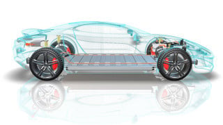
Monolithic step-down regulators combine a compact layout, high efficiency, and ultralow EMI for automotive environments.
Easy Layout and Ultralow EMI Silent Switcher 2 with High Efficiency
LT8640S/LT8643S are 42 V, 6 A continuous/7 A peak current monolithic step-down regulators featuring the second-generation Silent Switcher® 2 architecture. Silent Switcher regulators suppress EMI emissions by splitting the high-frequency hot loop in two—the split loops produce mutually canceling magnetic fields. The second-generation Silent Switcher 2 integrates bypass ceramic capacitors inside the package. These capacitors lie within fast ac loops (VIN, BST, and INTVCC) and would otherwise require precise and repeatable PCB layout to ensure EMI performance. Integrating them greatly simplifies PCB layout and manufacturing requirements. Even a low-cost 2-layer board can now exhibit exceptional EMI performance.
In automotive applications, designers prefer power supplies with a 2 MHz or higher switching frequency to avoid the AM frequency band and minimize solution size. Unfortunately, high switching frequency usually equates to lower efficiency and higher power dissipation, forcing designers to trade-off small size and low EMI performance against efficiency. The LT8640S and LT8643S eliminate this trade-off: they are capable of high efficiency and low power dissipation even at high switching frequencies, thanks to controlled, fast clean switching edges.
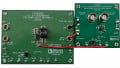
Figure 1 shows an ultralow EMI and high efficiency LT8640S 12 V to 5 V/6 A design. The internal regulator is supplied from the 5 V output through BIAS pin for lower power dissipation. This design is programmed at 2 MHz. The spread spectrum mode is enabled (SYNC/MODE = INTVCC) to allow the switching frequency to vary from 2 MHz to 2.4 MHz with 3 kHz triangular modulation.

Figure 1: Ultralow EMI LT8640S 5 V/6 A step-down converter with Spread Spectrum mode.
Figure 2 compares EMI emissions for 2-layer and 4-layer boards for the design of Figure 1. Both boards meet the stringent automotive CISPR 25 Class 5 radiated EMI specification using only a ferrite bead at the input side. Figure 3 shows efficiency. With switching frequency as high as 2 MHz, the LT8640S 12 V input peak efficiency reaches 95% and 24 V input peak efficiency reaches 92%.
Multiple LT8643S devices can be paralleled to support more than 7 A (peak) output current. The LT8643S utilizes current-mode control with external compensation to allow balanced current sharing—critical in a parallel configuration. Current sharing is naturally implemented by connecting all the error amplifier output VC pins together. The CLKOUT and SYNC/MODE pins enable frequency synchronization without additional clock devices.

Figure 2: CISPR 25 radiated EMI emission comparison between 2-layer and 4-layer boards using the Figure 1 design.

Figure 3: LT8640S 5 V/6 A output efficiency using Figure 1 design (fSW = 2 MHz).

Figure 4 shows an LT8640S design with 9 V output. Figure 5 shows thermal results at 5 A load. With 45 W output power and 1 MHz switching frequency, the LT8640S 4 mm × 4 mm LQFN package temperature rise is below 50°C, due to enhanced thermal technology.

Figure 5: LT8640S 24 V to 9 V/5 A thermal picture using Figure 4 design (fSW = 1 MHz, TA = 25°C).

Figure 6 shows the simplicity of a paralleled 12 V to 3.3 V/12 A LT8643S design. The top LT8643S is set to forced continuous mode by floating the SYNC/MODE pin; its CLKOUT signal drives the bottom LT8643S SYNC/MODE pin for synchronization. Figure 7 shows the efficiency of this design, while Figure 8 shows the 8 A step transient response.
Conclusion
LT8640S and LT8643S are 6 A (7 A peak) synchronous, ultralow EMI monolithic switching regulators in a small, 4 mm × 4 mm LQFN package. The patented Silent Switcher 2 architecture ensures remarkably low EMI emissions. The integrated hot-loop capacitors eliminate.
PCB layout sensitivity, which saves design effort and solution cost. Synchronous design and fast switching edges improve efficiency at heavy loads, while the light load efficiency benefits from low quiescent current. A wide input range of 3.4 V to 42 V and low dropout allow the LT8640S and LT8643S to meet the demands of automotive cold crank or load dump scenarios.

Figure 7: LT8643S 12 V to 3.3 V, 8 A step load transient using Figure 6 parallel design (fSW = 1 MHz).

Figure 8: LT8643S 12 V to 3.3 V/12 A efficiency using Figure 6 parallel design (fSW = 1 MHz)
About the Author
Ying Cheng graduated from Missouri University of Science and Technology (formerly University of Missouri-Rolla) with a Ph.D. in electrical engineering. She has been with Linear Technology (now part of Analog Devices) for six years as a senior applications engineer in the Power Products Group, working on dc-to-dc switching regulators and LDOs.
This article originally appeared in the Bodo’s Power Systems magazine.