Facebook
 Google
 GitHub
 Linkedin
Hard Paralleling SiC MOSFET-Based Power Modules
The main reasons for paralleling modules are technical and these reasons become more important with SiC MOSFETs for several reasons.
Perhaps the most fundamental question concerning this topic is to ask why parallel modules? What is the advantage of paralleling 2 x 200A modules to make a 400A module, why not simply use a 400A part? On the commercial side, in the 1200V class, IGBT modules are available in multiple current ratings and packages up to 3600A.
For SiC MOSFETs the options at higher currents (>400A) are much more limited, especially if industry-standard packages or multiple sources are required. Also, physically smaller packages that are manufactured in high volumes often can be produced at a lower cost than mechanically larger lower production volume packages.
However, the main reasons for paralleling modules are technical and these reasons become more important with SiC MOSFETs than with IGBT’s for several reasons:
- Multiple packages can be spread out on a heatsink and improve cooling. This allows more current to be delivered from what are more expensive SiC MOSFET modules.
- Larger physical packages have higher inductances in both the power loop and the gate driver circuits due to mechanical spacing and the use of screw terminal connections used to carry the higher currents.
- Using a large number of chips makes internal symmetrical layout and equalization of gate inductance for all the chips very critical and hard to optimize with packages that have limited terminal options.
- The two previous points enable faster switching speeds and hence lower switching losses and lower voltage overshoots during turn off to be achieved with these smaller packages.
Paralleling Differences Between IGBT’s and SiC MOSFETs
On closer examination, despite their fast switching speeds when it comes to paralleling SiC MOSFETs, they have some advantages when compared to IGBTs.
- SiC MOSFETs typically have a higher Rdson positive temperature coefficient, when compared to a Si IGBT VCE sat characteristic. This acts as negative feedback during static current sharing. If one device is taking more current those chips or modules, get hotter increasing the Rdson and hence reducing the current. This negative feedback reduces the level of thermal imbalance.
- Si IGBTs show a large increase in switching losses with increasing temperature and this has a positive feedback effect on temperature imbalance. A hotter chip has higher losses so getting even hotter. SiC MOSFETs show a very small increase in switching losses with temperature significantly reducing this effect.
- SiC MOSFETs have a softer transconductance curve meaning that small changes in gate voltage, when operating in the gate threshold region, have a smaller effect on drain current than an equivalent Si IGBT. This aids in dynamic current sharing.
- A statistical analysis of the Infineon trench gate devices shows that in terms of parameter distribution, modules with a higher RDS on have a lower switching losses which helps to match losses part to part.
Experience with a Paralleling Test Platform We will consider several aspects of this design platform.
- Module internal layout
- Power PCB layout
- Gate driver circuit design
- Gate driver PCB layout
- Instrumentation
- Static current sharing performance
- Dynamic current sharing performance
Internal Layout
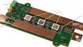
Paralleling must start with consideration of the module internal power and gate layout. The internal chip layout and module pinout can be designed to provide equal and symmetrical power and gate driver layout for the multiple chips in parallel. This is achieved while also keeping a low inductance layout switching loop inductance. In general, the pin grid array of style of PCB based modules allows the flexibility to optimize the layout.

Figure 1: Paths for current flow with a common auxiliary source connection
Power PCB Layout
For the power layout, the module is divided into two symmetrical halves. To match this symmetry the power layout was made as a mirror image down the centerline like butterfly wings. This is required to keep equal current sharing among the chips internal to the module. An exact facsimile of the layout was used for each of the four modules to keep current sharing between modules equal. It is also important to keep the external switching loop inductance low and this is achieved by overlapping the DC+ and DC- bus connections with multiple PCB copper planes and using local decoupling capacitors.
Gate Driver Circuit Design
When using a common gate driver circuit for all 4 modules with multiple gate connections, it is important to reduce any currents flowing in the auxiliary source connection. Figure 1 shows, in a simplified example of two modules, how the auxiliary source connection offers a natural parallel conduction path to the main current path. Some electrons which we call them “teenager electrons” because they like to take a different path from everyone else, can flow in this auxiliary source parallel path. This current can be large enough to cause gate oscillations and even fuse open the module internal auxiliary bond wires.
The circuit shown in Figure 2 was used to reduce these unwanted circulating currents. It is a combination of a common mode choke, which shows low impedance to normal gate currents where the in and out currents are equal, but high impedance to unwanted source currents flowing only in the source connection. In addition to this, a separate local boost stage was used for each pair of device gate connections. This allows for resistance in the source connection, but, with local capacitors, any current flowing in this path does not affect the gate waveforms. This is not the case if only a simple source resistor is used as any current flowing in that source resistor affects the gate source voltage which reduces the level of direct control and increases the potential for gate oscillations.

Figure 2: Gate Driver Circuit
Gate Driver PCB Layout
The 6 mΩ module has dual gate source pins and dual power drain and source connection points to reduce inductance and improve current sharing amongst the SiC MOSFET chips internal to the module. The first challenge of the gate layout is to have a symmetrical layout for both pairs of gate source connections.
After this is it key to turn on and off the gates of all four modules at the same time. The “tree” structure achieves this with low inductance trace gate/source pairs with similar lengths. Also for the local boost stage for each pair of gate source connections the layout was symmetrical. Measurements showed a worse case timing skew of less than 5nS difference between the gates during switching.
Instrumentation
Figure 3 shows the schematic used for the Double Pulse Testing (DPT). It is important to measure the current sharing with the topology set up as an as an H bridge so that the current flows and magnetic fields match the final application. Also, it is required to have the capability to generate synchronous rectifier switching pulses for the complementary device under test with dead times that meet the system dead time requirements.

Figure 3: Double Pulse Test (DPT) Schematic
To measure the drain and source currents, the DC bus PCB traces were laid out with holes on both sides to allow the use of a Rogowski coil. These are allowing the measurement of the current in the DCbus, which is the source current of the lower switch, and the DC+ bus current which is the drain current of the upper device. Also allowance was made to be able to measure the output current balance between the two sets of module output pins

Figure 4: DPT Current Waveforms for 4 Paralleled Modules (50 µs/ division and 50 A/division) Green Vgs 5 V/division. Blue Vds 100V/division

Figure 5: DPT Current Waveforms for 4 Paralleled Modules (50 µs/ division and 50 A/division)
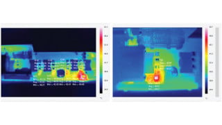
Static Current Sharing
Figure 4 shows the source current in the four lower devices during a DPT. Synchronous rectification was used after the first pulse to turn on the upper SiC MOSFET, following the dead time; but, not after the second pulse which allows the current to free wheel through the upper body diode. Current sharing of four matched modules was +/- 3%. Note that the current sharing is worse after the second pulse when the MOSFET is not gated and only the body diode is conducting current.

Figure 6: DPT Turn-off Waveforms for 4 Paralleled Modules (200 ns/ division and 50 A/division) Green Vgs 5 V/division. Blue Vds 100V/division

Figure 7: DPT Turn-on Waveforms for 4 Paralleled Modules (200 ns/ division and 50 A/division) Green Vgs 5 V/division. Blue Vds 100V/division.
This initial test was done with modules selected to have an RDS on variation of less than 2%. Tests were also performed with modules with a 7% RDS on variation and the sharing was only marginally worse at +/- 4%. Additional testing at high temperature and switching upper devices showed equally good performance. Figure 5 shows an expanded view of the current waveform in Figure 4.
Current sharing in lab vs high volume production
So excellent current sharing has been shown in the lab with a very small sample. However, if this design has to be translated into a high volume commercial product, current sharing for randomly selected modules with their normal distribution of electrical parameters must be calculated. The method used for this is referred to as a Monte Carlo analysis named after the famous casino in Monte Carlo. A set of four modules are selected (each one randomly) from the statistical production spread of RDS on and switching losses values. Using these parameters for each module, the current in each module is calculated and the junction temperature estimated. As the RDS on and switching losses are temperature dependent, an iteration is used to calculate the final current and junction temperature of each module. This process can be repeated for say 50,000 sets of randomly selected modules and the normalized distribution of Tj calculated. In this case, the results was a variation at +/- three sigma of +/- 7C. Another wrinkle in the calculation is that there is a cross correlation between RDS on and switching losses Etot where parts with a lower RDS on trend to a higher Etot value.
Summary
This article has shown that four modules can be paralleled with excellent current sharing in both static and dynamic operating conditions and with a Monte Carlo analysis parts can be selected at random and still achieve good sharing for volume production. Care must be taken with the gate driver auxiliary circulating currents and of course engineers must follow the three most important design rules when paralleling power semiconductors namely symmetry, symmetry and symmetry.
References
- Infineon AN 2017-41. Evaluation Board for CoolSiC™ Easy1B halfbridge modules.
- Infineon AN 2017-04. Advanced Gate Drive Options for silicon carbide (SiC) MOSFETs using EiceDRIVER™.
- Infineon AN2014-12. EiceDRIVER™ 1EDI Compact Family. Technical description.
- Infineon AN2018-09. Guidelines for CoolSiC™ MOSFET gate drive voltage window
- Infineon AN2017-14. Evaluation Board EVAL-1EDI20H12AH-SIC.
- Infineon AN2007-04. How to calculate and minimize the dead time requirement for IGBT’s properly.
- Infineon AN2017-46. CoolSiC™ 1200 V SiC MOSFET Application Note
This article originally appeared in the Bodo’s Power Systems magazine.
About the Authors
Andre Lenze is the Technical Marketing Manager at Infineon in the Industrial Power Control division. There he oversees the CoolSiC Easy module product family. Lenze studied industrial engineering at the Fachhochschule Südwestfalen-Soest with a focus on electrical engineering, marketing, and sales.
David Levett works at Infineon Technologies as a Power Electronics Design and Application Engineer. He is responsible for the application and design for power electronics in machines, planes, and other technical disciplines from gate drive design, stack protection, mechanical assembly, thermal system evaluation to EMI mitigation. Levett enjoys conceptual designs and design reviews as well. He is particularly skilled in the field of power electronics and design, as well as grid-tie power converters in solar, wind, and battery. He earned his Ph.D. in Electrical Engineering at the University of Southampton located in England.
Ziqing Zheng
Krzysztof Mainka