Facebook
 Google
 GitHub
 Linkedin
Fully-Protected Half-Bridge Power ICs Enable Motor-Integrated Inverters
Navitas’ GaNSense technology provide size and loss savings to enable integration of the inverter with the motor.
Motor drives consume nearly 50% of the electricity produced in Europe [1]. Governments have therefore created regulations and standards to make sure electricity is consumed as efficiently as possible with the least impact and disruptions to the electrical supply grid. Variable speed drives (VSD) are now common in the industry as they reduce energy usage up to 90% compared to older constant-speed induction motors [2], whilst having the added benefits of reduced motor size, improved dynamic performance and reliability.
Standards such as IEC 61000 were created to support the electrical supply grid in terms of immunity and emissions of electrical equipment, as large inductive loads presented by motor drives can significantly impact local-grid stability. To address these standards, various techniques have been implemented in the motor-drive system, including active power-factor correction (PFC), which modulates the distorted wave back into a sinusoidal wave to maximize real power from the grid supply.
GaN Improves Both Performance and Cost
Gallium nitride (GaN) is a wide-bandgap semiconductor which offers superior characteristics compared to older silicon equivalents, including the ability to switch up to 20x faster and increase power density by over 3x times. Implementing GaN power devices into a motor-drive system for PFC and inverter stages provides a significant reduction in power losses, and size, enabling the integration of the inverter with the motor. In this article, a 400 W reference design for a motor integrated inverter created by Navitas is explained in detail.
GaN FETs do not have any reverse recovery charge, which allows for extremely fast switching, resulting in 4-5 x lower switching losses than silicon IGBTS and MOSFETs and approximately 50% reduction in total power losses. This reduction in power translates to reduced dissipated heat from the device, allowing heatsinks to be reduced in size - or even eliminated in lower power drives. In 2021, the cost of heatsink-grade machined aluminum reached a 13-year high, with a price of around $8/kg, so minimizing heatsink requirements allows significant savings on the total system cost. In addition, lower shipping costs result due to reduced system weight.
The combination of extremely low switching losses and no reverse recovery enables a new degree of freedom in switching frequencies, but also thermal design for VSDs. Motor-integrated inverters have difficult operating conditions, apart from vibrations and strong magnetic fields the ambient temperature can be quite elevated, making cooling of the power semiconductors tricky, so it is best to start off with a power switch that does not produce a lot of heat to begin with.
Integration Improves Efficiency, Control, and Robustness for Motor Drives
GaNSense technology integrate the performance of GaN power with driver, protection, and dynamic-sensing capabilities, making them ideal for high-reliability motor-drive applications. The optimized gate-drive circuit with associated voltage regulator and protection circuits, such as over-temperature and over-current detection has the autonomous ability to self-protect. All these features are fully integrated, resulting in the superior performance with highest reliability. The input signal can be controlled with a simple digital signal, eliminating external components, and reducing PCB area. This becomes beneficial for compact motor drives, where the complete electronic system can fit in the motor housing.

Figure 1. Simplified block diagram of a fully integrated GaNFast IC with GaNSense technology from Navitas. Image used courtesy of Bodo’s Power Systems [PDF]
Compared to discrete silicon or discrete GaN approaches, GaNSense™ technology can ‘detect and protect’ in only 30 ns - 6x faster than silicon or GaN discretes, improving system-level reliability. More details are explained in Application note AN015.
Integration of temperature control on the power switches offers higher precision and real-time sensing compared to a traditional low-precision temperature sensor on a heatsink. This is critical for motor-integrated drive applications that cannot easily be serviced, and where – especially in industrial settings – highest reliability and uptime are expected. The built-in over-temperature protection circuit will turn off the GaN IC when set temperatures are exceeded, enabling fast protection of the system.
The benefit of loss-less current sensing in GaNSense technology eliminates the need for large and expensive shunt resistors, significantly reducing system size and cost, whilst maintaining fast overcurrent protection for system robustness as required in industrial motor drives for factory automation.
Additionally, the total component count is lowered, yielding a significantly lower FIT (failures in time) rate and improvement in system reliability. Navitas recently announced a 20-year limited warranty on its products, which is an industry first to highlight their exceptional reliability.
Navitas is introducing a full family of GaN power ICs in half-bridge topology, as can be seen in table 1. As multiple different GaN power half-bridge ICs with different RDSON values exist that are pin-compatible, the design is easily scalable up or down in power.
Table 1. GaN power IC portfolio in half-bridge topology from Navitas
| Part # | Type |
VDS(CONT) (V) |
VDS(TRAN) (V) |
RDS(ON) (mΩ, typ) |
Package | Status |
| NV6247 | Half-Bridge | 650 | 800 | 160/160 | PQFN 6x8 | Production |
| NV6245C | Half-Bridge | 275/275 | PQFN 6x8 | Engineering |
All the new half-bridge products come in space-saving PQFN packages for very good thermal connection to the PCB and low parasitic inductance and resistance, and show the same robustness and reliability as Navitas’ single power switches, in particular high transient voltage capability (650V continuous, 800V transient). They are covered by the recently announced 20-year warranty. Further information on the performance and robustness of the products can be found in their respective datasheets [3] and dedicated Application Note AN-018 at www.navitassemi.com [5].
Reference Design for Motor-Integrated Inverter
The availability of GaN power ICs in half-bridge topology enables the implementation of very compact motor inverters, as shown in figure 2.
This inverter consists of three half-bridge GaN power ICs from Navitas, the new NV6247. It contains the input logic, level shifter, voltage regulators and gate drivers, and the current and temperature sense circuits, as well as the bootstrap supply. As a result, the external component count is very small.
The schematic for one of the three legs of the inverter is shown below in Figure 3. Shown is the circuit for the second phase, with all three phases being identical. The main component is the NV6247, integrating the two power switches in half-bridge configuration, as well as the gate drivers and their regulators, and the input logic labeled “PWM”. A built-in bootstrap circuit is used to provide the gate drive power to the high-side driver. Also included is a level shifter, so that the input signals can be ground-referenced, making this device a digitally-controllable power stage in the best sense of the word.

Figure 2. Circular PCB with a 400W motor inverter power stage that attaches to the back of a BLDC motor, with a diameter of 56mm. Image used courtesy of Bodo’s Power Systems [PDF]
Furthermore, several sensing functions are included. First, the current flowing through the internal low-side GaN power FET is sensed internally and then converted to a current at the current sensing output pin (CS). Second, the junction temperature is sensed with a circuit on the gate driver and used to turn off the power switches when too hot.
The IC pins include the drain of the high-side GaN power FET (VIN, connected to VBUS), the half-bridge mid-point switched node (VSW, connected to PHB), the source of the low-side GaN power FET and IC GND (PGND), low-side IC supply (VCC), low-side gate drive supply (VDDL), low-side turn-on dV/dt control (RDDL), low-side 5V supply (5VL), low-side referenced PWM inputs (INL, INH), low-side current sensing output (CS), auto-standby enable input (/STBY), high-side supply (VB), high-side gate drive supply (VDDH), and high-side 5V supply (5VH). The external low-side components around the IC include VCC supply capacitor (CVCC) connected between VCC pin and PGND, VDDL supply capacitor (CVDDL) connected between VDDL pin and PGND, turn-on dV/dt set resistor (RDDL) connected between VDDL pin and RDDL pin, current sense amplitude set resistor (RSET) connected between CS pin and PGND, 5V supply capacitor (C5VL) connected between 5VL pin and PGND, and auto-standby enable pin (/STBY) connected to PGND to enable auto-standby mode or connected to 5VL to disable auto-standby mode. The external high-side components around the IC include VB supply capacitor (CVB) connected between VB pin and VSW, VDDH supply capacitor (CVDDH) connected between VDDH pin and VSW, and 5V supply capacitor (C5VH) connected between 5VH pin and VSW. The high side VB, 5VH and VDDH bypass capacitors must be chosen carefully to accommodate various system considerations such as high side wake up time, high side hold up time and standby power. On the right side, the VBUS blocking caps can be seen, and the PCB allows the use of film or electrolytic caps. Their purpose is to dampen any kind of ringing that might occur because of parasitic inductance in the supply and the switching action, since the board is designed for DC input. Finally, R17 and C18 can be used to dampen ringing on the switch nodes, as it might be caused by long cables and their inductance, and are optional.
It is important to note that the switching speed of the power switches can be adjusted with an external resistor (R7 in this case). While slowing down the switching speed does increase switching losses, the impact is not large as the switching losses are very low to begin with. That way, the switching speed can be adjusted to whatever the motor needs, and the resulting EMI can be tuned to comply with all required regulations and EMI filter components can be downsized. A value of 50Ω is a good starting point.

Figure 3. Schematic of one of the three inverter legs, showing that in addition to the GaN power IC very few external components are needed. Image used courtesy of Bodo’s Power Systems [PDF]
The resistor on the CS pin (R8) can be set as needed by the microcontroller and its ADC input, to scale the voltage appropriately. However, If the voltage on this pin exceeds 1.9V, the overcurrent protection is triggered. It needs to be noted that the choice of the resistor on the CS pin will affect both the voltage corresponding to the current in the power stage, as well as the overcurrent protection.
The auto standby mode is designed to reduce the power consumption of the NV6247 when it is not switching. If no more input pulses are detected for a time longer than ~90 µs, the IC will automatically enter low power standby mode. This will disable the gate drive and other internal circuitry and reduce the VCC supply current to a low level. When the INL pulses restart, the IC will wake up after a delay (typically around 450ns) at the first rising edge of the INL input and enter normal operating mode again.
Performance Results
The inverter has been designed and built in Navitas application engineering labs, and full design documentation will be made available. It has been tested along with a BLDC motor and mechanical load under the following operating conditions: DC input voltage 300 V, ambient temperature 25°C, FOC (field oriented control) algorithm with a switching frequency of 20 kHz. The thermal resistance from PCB to ambient has been measured with ~12.5 K/W. Figure 4 shows the resulting inverter efficiency (electrical output power versus input power, not considering the motor efficiency), which is approaching 99% for output power of 300 W. While the efficiency of the inverter usually is much better than the motor efficiency, it is still important to understand the losses produced in the inverter, in order to design the cooling system accordingly. With a power dissipation of <3W at full load, the heatsink can be reduced a lot, and the thermal design of the system is much easier, eventually avoiding a lot of manual assembly work usually associated with attaching large heatsinks. The two curves shown correspond to different settings for the slew rate (red = 20 V/ns, blue = 40 V/ns), the difference being rather small.
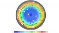
Figure 5 shows the temperatures across the PCB while operating the inverter at an output load of 300W. With ambient temperature of 25°C, the package surface temperature stays below 60°C, not surprising given the very low losses. As the PQFN power switches are thermally well connected to the PCB, the maximum power output is thermally limited by the allowable PCB temperature, usually 105°C. The GaN power switches themselves do tolerate much higher temperatures, and as a result this design offers both exceptional reliability as well as great robustness for abnormal operating conditions like output short-circuit or rotor stall, that may drive the power switch temperature up very quickly until the controller or the built-in overtemperature protection circuit can react.

Figure 4. Inverter efficiency across the whole output power range is approaching 99%. Image used courtesy of Bodo’s Power Systems [PDF]

Figure 5. Thermal scan of the inverter board, showing the comparatively low surface temperatures due to the low losses of the inverter. Image used courtesy of Bodo’s Power Systems [PDF]
GaNSense Half-Bridge ICs
Every motor has different requirements, but the trends are in the same direction: improved efficiency, better performance, and lower cost. GaNSense half-bridge ICs enable higher system efficiencies and improve performance, while reducing total cost of ownership of the complete system. GaNSense half-bridge ICs offer the highest level of integration - drive, power, protection, and sensing to enable motor-integrated inverters with great performance and reliability.
This article originally appeared in Bodo’s Power Systems [PDF] magazine.