Facebook
 Google
 GitHub
 Linkedin
Double Pulse Testing
Two or double testing is a key implement in the toolbox of power electronics engineers that enables comprehensive and accurate measurements to be made early in the design cycle, reducing time to market.
Introduction
Testing the switching performance of power semiconductors in a safe and controlled environment is a challenge. Unforeseen problems that will come up during the project. Now the famous bard once wrote, “many a true word hath been spoken in jest” (1), and the reality is that unforeseen technical issues can put any project months or even years behind schedule. This is especially true if these occur late in a project.
The earlier in any project technical issues can be identified the less impact they will have on the overall project timeline. So what has this to do with Double Pulse Testing (DPT)? Amongst the many benefits of DPT, the most valuable is the ability to test a power stack under worst-case corner operating conditions early in the design cycle and so reduce the risk of unforeseen problems popping up later in the program timeline.
A DPT is a tool that enables a power switch to be turned ON and OFF at different current levels as shown in figure 1. By adjusting the switching times T1, T2, and T3 the turn ON and turn OFF waveforms of the Device Under Test (DUT) can be controlled and measured over the full range of operating conditions.

Figure 1: Double pulse waveform
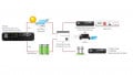
Test Setup Circuit
Figure 2 shows a typical circuit diagram for a DPT experimental setup. Here the DUT, which is a SiC MOSFET, device 2 the lower-left device in the “H” bridge, is instrumented so that the source current, drain to source voltage, and gate to source voltage can all be measured while the device is switched. The switching times T1, T2, T3, and hence, currents can be adjusted using a programmable pulse generator. The complementary SiC MOSFET, device 1, is also switched for synchronous rectification operation. A load inductor limits the rate of di/dt. The key considerations for the selection of this inductor include:
- It should not saturate at the peak test currents.
- It should limit the di/dt so that the switching times (T1, T2, and T3 in figure 1) are not less than 10 μs, to ensure the devices have fully turned ON or OFF.
- The di/dt should not be so low that the switching times are longer than 200 μS so as not to cause the DC bus voltage to dip by more than ≈5 percent, and so change the switching performance. In addition, if the current pulse is long, then the chip temperature can increase by more than a few °C, again affecting the switching performance.
- The inductor should be mounted well away from the test setup to prevent EMI interference or magnetic field coupling into any gate drive circuits or instrumentation.

Figure 2: Typical DPT circuit diagram
The DC bus voltage level can be adjusted using a variable DC supply. Some frequently asked questions are:
Why the second pulse? It is important to build up current in the complementary device or diode so that when the switch turns on, the effects of any reverse recovery current can be evaluated.
Why is the configuration an H bridge as shown in Figure 2? Can a single half-bridge be used with the load inductor connected to either DC + or DC -? An H bridge is shown in Figure 2 as in many applications the load is switched between two half-bridges and so this topology is a representative implementation of the final system. However, a single half-bridge topology with the load inductor connected to either DC bus rail is simpler and will provide accurate results for most operating conditions. It is recommended that the full H bridge be used when testing modules in hard parallel. This H bridge can also be useful for evaluation of device performance under phase-to-phase short circuit conditions or under short circuit type 2 events depending on the customer application requirements.
Can this be used to test a three-level topology? Yes. This is shown in more detail later in this article.
Why is the DC minus supply connected to the ground? In this case when measuring a lower device and using a “floating” DC bus power supply the DC minus supply can be grounded allowing instrumentation to be grounded and the use of single-ended voltage probes rather than differential probes.
How: Safety
It is hard to over-emphasize the importance of safety when performing a DPT: high voltages can be lethal. Safety is critical during double pulse testing. Lethal voltages are often present and when components fail, the results can be dramatic and lead to the ejection of hot materials. For this reason, it is strongly recommended that the high voltage portion of the test setup be enclosed inside a protective cover (figure 3). This barrier can work both directions, keeping unwanted materials out, for example, a hand or cup of coffee, and keeping unwanted materials in, such as electrolyte from a failed capacitor.

Figure 3: Example of a DPT enclosure
An additional layer of security can be added for the “distracted” operator by having a warning light when high voltage is present and an interlock on any access door, which, when opened will immediately cut power and discharge any high voltage capacitors.
Following are some suggested rules to be taken under serious consideration:
- Follow all company and lab health and safety guidelines.
- Always keep all high voltage components within a safe enclosure. A test enclosure can protect from accidental contact with high voltage circuits and provides a physical barrier during potential dramatic failure events.
- Disconnect high voltage supplies and discharge any high voltage capacitors before accessing high voltage circuits inside the enclosure. The addition of a permanent discharge resistor can provide another layer of safety.
- Use correct grounding for instrumentation. Employ safe methods to measure upper devices (e.g. differential probes). Ensure a good low impedance ground connection to the module mounting plate and enclosure metal structure or surfaces.
- In case of a module failure, ensure that the high voltage DC supply has a current limiting feature or fast-acting fuses to limit fault energy.
- Never work alone when high voltages are present.
- Ensure all equipment users have received correct safety and first aid training.
- Ensure the equipment has a clearly marked and easily accessible emergency power OFF button.
As shown in Figure 2, it is possible to ground the DC minus when measuring the lower devices and so have instrumentation at safe ground potential. For measurement of upper devices, isolated current sensors and differential voltage probes must be used enabling the scope to operate at safe ground potential.
It is good to use the ”buddy” principle in the event of an incident so someone is available to provide cardiopulmonary resuscitation and call for emergency aid. Finally, if high-temperature chip switching tests are being performed, components surfaces can be at temperatures >50 °C and so cause burns. Caution is required.

Figure 4: Voltage probe tip to reduce inductance in the measurement loop
Instrumentation
To measure the DUT voltages as shown in Figure 2, it is possible to use single-ended probes. Figures 4 and 5 show some techniques to reduce loop inductance and coupling in the measurement path and how some turns around a ferrite core can add common mode impedance to the measurement signal. To measure voltages at nonground reference potentials, differential probes are required and should be selected with a high common-mode rejection ratio, as the DUT can be moving at very high dv/dt levels with respect to the scope ground. Ensure that all voltage probes have the required voltage rating.

Figure 5: Voltage probe with some added common-mode impedance
To measure the actual device switching current, a current sensor must be inserted into the collector/emitter or source/drain of the DUT. This can be a challenge as accuracy is required but it is important not to add a large amount of loop inductance which would distort any results. Typical methods include; but, are not limited to:

Figure 6: Rogowski coil fitted around the terminal of a 62 mm module
Pearson current sensors (2): These have very high bandwidth and accuracy. However, they have the disadvantage of being large, so making it difficult to insert into the power circuit without increasing the loop inductance. They also have a metal case that can make it problematic to isolate from live bus bars etc.

Figure 7: Rogowski coil fitted around a standoff fitted into the terminal of an EconoDUAL™ 3 module
Rogowski coils (3): These have a bandwidth of between 15-30 Mhz which is enough for many applications and any delay skew can be compensated for with an oscilloscope. They have the advantage of being flexible and so are easy to insert into the power circuit. Figures 6, 7, and 8 show them used on a 62 mm, EconoDUAL™ 3 with small standoffs and a PrimePACK™ module. In case it is needed, do not be afraid to cut a little plastic to help to get the coil to fit. Some high power modules have more than one screw connection for the collector or emitter current and in this case, more than one probe might be required. Figure 9 shows how a coil can be used on a PCB based design with a loop around a current-carrying trace. This method requires that the PCB designed with this end in mind.

Figure 8: Rogowski coil fitted around the terminal of a PrimePACK™ 2 module
Figure 10 shows a typical Pearson and Rogowski current sensor. Current shunts can be used especially on low current devices where they can be fitted into a circuit without significantly increasing the loop inductance.
Three-Level Topology
DPT of a three-level topology requires additional consideration. Working with Figure 11 as a reference of a Neutral Point Clamp (NPC) I topology, the switching patterns are described in Table 1. Test sequence 1 shows a switching sequence between the neutral point and DC-. Test sequence 2 shows a switching sequence between the neutral point and DC+. To measure the opposing devices the load inductor can be connected between the output and DC+ and a complementary switching sequence used. Note S1 must always be turned off before S2 to avoid the full bus voltage being applied across S1.

Figure 9: Rogowski coil used to measure current in a PCB trace
What testing should be included in a DPT It has been shown how the DUT can be switched at different voltages and currents. A third key parameter that affects the switching characteristics of a power semiconductor is temperature. This can be adjusted by mounting the DUT on a plate, which can be heated or cooled. For testing at temperatures lower than 0°C, which can be achieved with a chill plate and freezing water, the test setup can be installed inside an environmental chamber and the temperature reduced to -20°C or -40°C as the application dictates.

Figure 10: An example of a Pearson (abpve) and Rogowski coil (below) current sensor

Figure 11: NPCI topology. For test sequence 1 current shown in green for time periods 1 and 3 and blue for time period 2
With this set of three variables, the DUT can be operated at the key corner operating points, for example, maximum bus voltage, maximum current but low operating temperature. This combination can produce the highest voltage overshoot during turn off, and so is critical to ensuring the DUT remains within its RBSOA. It is recommended to measure both the active switch and any complementary diode under this range of operating conditions.
Table 1: Test switching pattern.
| Test Sequence |
Time Period |
Switches that are Commanded On (All Other Switches are Commanded Off) |
Devices that are Conducting Current |
| 1 | 1 (Pulse 1) | S2 | S2 and D5 Green |
| 2 | None | D3 and D4 Blue | |
| 3 (Pulse 2) | S2 | S2 and D5 Green | |
| 2 | 1 (Pulse 1) | S1 and S2 | S1 and S2 |
| 2 | S2 | S2 and D5 | |
| 3 (Pulse 2) | S1 and S2 | S1 and S2 |
Apart from corner conditions, several other tests should be considered.
- Short circuit and over current protection circuits both phase to phase and shoot through. Note care should be taken, especially with higher current power modules, as the high di/dt levels than occur during a short circuit event can cause magnetic field coupling from bus bars and cables into gate driver circuits, power supplies, and instrumentation.
- If the switch dv/dt needs to be limited below a certain level, as is often required in motor drive applications, the value of the gate resistor can be adjusted to meet the desired value.
- Accurate measurement of the device switching losses. Although the data-sheet is a good starting point for switch loss estimation, typically a design will differ from the operating conditions used to derive the datasheet values (4). These differences, for example in the gate driver and bus inductance, will produce different switching loss energies than those listed in the datasheet. Measuring these dynamic losses is important to estimate system efficiency and the maximum junction temperature of the power semiconductors.
- Measurement of the switching loop inductance, di/dt, and voltage overshoot to understand the factors involved in designing within the power device RBSOA.
- Measurement of the switching times can be used to evaluate the values for the dead or interlock delay time to prevent shoot-through events (5).
- In a half, bridge topology, check the upper device gate waveform in the off state when turning on the lower device to check for the possibility of a parasitic turn on due to the Miller capacitance.
- The sample size and device-to-device parameter variation is a difficult topic. It is very not realistic to measure say 100 devices and create a statistical analysis for all parameter variations from the results. It is recommended that engineers collaborate with their power semiconductor supplier to bound the scale of any variations and ensure that suppliers have a high level of consistency and quality in their production processes.
The Benefits of Testing
There is a considerable investment required to build a DPT setup and it is important to ask for a return on this investment. Some of the returns are that it is safer and faster to make measurements under turns are that it is safer and faster to make measurements under the controlled conditions of a DPT compared to making these same measurements in a final converter assembly where, for example, the junction temperature is difficult to control or measure.
Waveforms and test results can be stored as reference waveforms and if changes are required later in the design or during production these can be used as templates to evaluate the effect of any design modifications.
Accurate measurement of switching losses is critical for the estimation of the device junction temperature under worst-case operating conditions.
Having a standard test plan and setup helps all power converter designs to share a common qualification process.
As stated in the introduction, running these tests early in the design cycle and being able to solve any issues that arise can help keep any project on track.
Now a key and difficult question is when in the design cycle to perform this testing. Too early and the design is not representative of the final system and too late and there is a risk of an issue that can cause significant time delays to the program. Engineers should use good design judgment and try to perform the testing as early in the design cycle as possible.
It must be noted that DPT can cover most of a power semiconductor operating conditions, but it cannot fully emulate the operation of a full converter. Issues like noise pick up on control lines, software bugs, and effects of magnetic fields, all of which can affect the reliable operation of the power switches, will not be identified with this test. DPT does take time and design effort. However, this effort will provide a payback in terms of safety, accuracy, product reliability, and project timelines.
References
- William Shakespeare, King Lear, 1605
- Pearson current sensors web site.
- Rogowski coil web site.
- Infineon application note AN 2011-05 V1.2 November 2015: Industrial IGBT Modules Explanation of Technical Information pages 18 and 19.
- Infineon application note AN 2007-04: How to calculate and minimize the dead time requirements for IGBTs properly.
About the Author
David Levett works as a power electronics design and application engineer at Infineon. He received his Doctor of Philosophy (Ph.D.) in Electrical Engineering Motor Drives at the University of Southampton.
Ziqing Zheng received her Master's Degree in Power Electronics & Electric Drives at Shanghai Maritime University. She works as an application engineer at Infineon
Tim Frank works at Infineon in North America.