Facebook
 Google
 GitHub
 Linkedin
An Introduction to the Double-Pulse Test for Power MOSFET Characterization
This article alleviates the confusion surrounding double-pulse testing and offers a step-by-step double-pulse test setup.
This article is published by EEPower as part of an exclusive digital content partnership with Bodo’s Power Systems.
Over the last 20 years, I have heard many—sometimes amusing—explanations for the double pulse. For example, “the double pulse is the characterization of an electrical quadrupole, with the first pulse describing the input and the second pulse the output.” What is self-evident for the experienced professional can sometimes cause misunderstandings for the less experienced. As a test equipment manufacturer, we realize users have different perspectives on double-pulse testing.
The development of a power electronic assembly requires several steps. One of these involves the dynamic characterization of the switching behavior of the power semiconductors. For this purpose, a double-pulse test setup is used which includes:
- a capacitive energy storage device, also known as a dc-link capacitor,
- the power semiconductors that are to be tested, which consist of at least one switch and one diode, and
- a load inductor, which functions as a magnetic transducer.
The IEC 60747-9 standard explains the corresponding test setup and measurement results using the example of an IGBT. As expected, no further details about the real designs and possible pitfalls are given.
What Is the Double Pulse Used For?
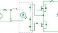
The schematic of a possible double-pulse setup is shown in Figure 1, with the measurement data in Figure 2.

Figure 1. Basic double puls setup, including two MOSFETs. Image used courtesy of Bodo’s Power Systems [PDF]

Figure 2. Simulation results of a double-pulse setup. Image used courtesy of Bodo’s Power Systems [PDF]
With a first pulse, the load inductance is magnetized up to the desired rated current, whereby switching off the current provides the first data (A) on the switch-off behavior at the operating point. After a recovery time, during which the semiconductor must be completely de-energized, it is switched on again. The previous nominal current flows - driven by the load inductance - in the opposite diode. When switched on again, the current commutates back into the semiconductor that is being tested.
This provides the second data set (B) with all the information about the turn-on behavior of the power semiconductor. The second pulse is switched off once the turn-on process is fully recorded under nominal current. However, the resulting data are not necessarily of interest.
Generally, it is assumed that a semiconductor that survives a switching operation at a specified operation point without any problems will always survive this operation point. Provided the semiconductor does not degrade, and the resulting heat is continuously dissipated. The required cooling capacity can be calculated by characterizing all plausible operation points and calculating the power losses, considering the switching frequency.

Figure 3. Saxogy´s double-pulse test box with temperature management and inert gas connections. Image used courtesy of Bodo’s Power Systems [PDF]
Parasitic Passives
In addition to the load inductance, each piece of connecting cable introduces further inductance into the circuit. Unfortunately, this also occurs in areas where there should be as little as possible or no inductance at all. Additionally, each piece of cable forms a coupling capacitance to neighboring conductors. These parasitic passive components, in turn, form resonant circuits, which fast-switching components easily trigger.
Of course, all distances between the components should be as short as possible. The commutation circuit, formed by the two semiconductors and the dc-link capacitance, can thus be reduced to inductance values of approximately 10 nH.
After the turn-off, the corresponding semiconductor turns off by building up a junction barrier. The junction capacitance forms a resonant circuit with the commutation inductance. The resulting turn-off oscillations can be recognized as an overlap on the reverse voltage curve. The turn-off process interrupts the current flow in the commutation inductor, causing it to generate a turn-off overvoltage.
Depending on the setup, the overlap of turn-off overvoltage and turn-off oscillation can lead to an increase or partial cancellation of the peak voltage value. The turn-off behavior should be characterized under worst-case conditions to prevent the maximum reverse voltage on the semiconductor from being exceeded and the associated destruction of the semiconductor. These include using the future target layout, the expected junction temperature with the highest switching speed, and the turn-off at the highest current.
Experience shows that critical conditions sometimes occur even at operating points between the maximum values. For this reason, close characterization of the switching processes over the entire operating range is recommended.

Figure 4. SAXOGY´s fully automated double puls test bench with included measurement equipment. Image used courtesy of Bodo’s Power Systems [PDF]
The Right Sequence Saves Time
Here, a fundamental distinction must be made between characterizing the semiconductor and characterizing the power electronics.
Load Current
The easiest and fastest way to obtain data is to modify the operating point of the current. The current to be switched off is related to the turn-on time. There are two issues to be considered:
a. The current-carrying load inductance has a certain amount of energy the dc-link capacitance provides until it is turned off.
b. Energy was lost during the turn-on phase due to conduction losses. As a result, after the turn-off, the dc-link capacitance no longer has the same voltage value as when it was switched on.
To switch off at a specific voltage value, the dc-link voltage must be increased by the expected difference. The current range should consider all values during operation - especially short circuit events.
The range between two operating points is debatable: 5 to 10 operating points within the rated current range are common. Of course, a fully automatic test bench allows a more closely meshed characterization. Fortunately, the days when every measurement plot was saved on a disc or evaluated with a lot of manpower are long gone.
Gate Configuration
Some setups offer the option of manipulating how the gate driver is controlled. For example, gate resistors, gate currents, or gate voltages can be adjusted automatically. As these directly influence the switching behavior, those must be considered during the characterization. Often, only seconds are needed to re-parameterize the gate driver. It is therefore recommended to include the new parameter in the characterization after each operating point or at the end of a series of operating points with the same dc-link voltage.
However, manual parameterization should occur at the end of the entire measurement series if the gate driver is not automated. As the test system must be disconnected from the power supply after each pulse and the statistical number of accesses is significantly higher than when parameterizing a complete series, this substantially minimizes the safety risk. Characterization over the entire current range is now repeated for different dc-link voltages. It is advisable to characterize several current values with the same dc-link voltage to save energy and time. This avoids unnecessary charging and discharging cycles of the dc-link capacitor.
DC-Link Voltage
The voltage range limitations for semiconductor characterization are between zero and usually 80% of the maximum permissible reverse voltage. The turn-off overvoltage must never exceed the maximum permitted reverse voltage!
For example, it is possible to limit the characterization parameters to the voltage range of the inverter when characterizing power electronics. Usually, all voltage ranges are measured with at least 5 to 10 intermediate points, whereby a more detailed characterization provides more insight.
Junction Temperature
The junction temperature is usually the last parameter to be modified. Several different methods are possible. The easiest way to control the temperature is to use a heating plate, where the semiconductor or the heat sink is heated to the desired temperature. However, this method makes only junction temperatures above room temperature possible.
An extension of the process is the temperature regulation utilizing a hydraulic temperature control plate. In principle, this is an oil-filled heat sink. A temperature control unit controls the temperature of the oil. This setup allows temperature ranges between -40°C and +200°C. It should be noted that condensation and later icing of the device under test (DUT) can occur at temperatures below the dew point. In turn, metallic surfaces can oxidize at high temperatures. Ideally, the DUT should be operated in an inert gas environment. The moisture and oxygen-free environment prevents both icing and oxidation.
Saxogy offers predefined double pulse and custom solutions.
This article originally appeared in Bodo’s Power Systems [PDF] magazine.