Facebook
 Google
 GitHub
 Linkedin
Design Considerations for a GaN-Based High Frequency LLC Resonant Converter
This article discusses the benefits of commercial GaN power transistors in comparison to Si SJMOS and SiC MOS transistors for a soft-switching LLC resonant converter.
Introduction
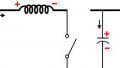
With the clear trends toward higher power, smaller size, and higher efficiency, a high frequency LLC resonant converter is an attractive solution for an isolated DC/DC topology in the industry, such as a laptop adapter (>75W), 1KW-3KW datacenter Power Supply Unit (PSU), and a multi-kilowatt On-Board Charger (OBC) for electric vehicles. Figure 1 shows a topology for a half-bridge LLC resonant converter with switching frequency at 100KHz and 500KHz. At the higher frequency, it is obvious that the size of the passive resonant tank (e.g. transformer, resonant inductor, and resonant capacitor) is dramatically reduced, thus the power density is improved.
Additionally, the selection of the power transistors (Q1 and Q2) need to be considered to trade off the efficiency and power density. GaN power transistors have established themselves in the market as a proven transistor technology, but are often not considered in soft switching applications. While using GaN in hard switching applications shows a significant improvement in efficiency, improvements on efficiency and frequency in soft-switching converters (such as LLC) can also be equally dramatic.

Figure 1: The Half bridge LLC resonant converter at 100KHz and 500KHz
In this article, the benefits of commercial GaN power transistors in comparison to Si SJMOS and SiC MOS transistors are discussed for a soft-switching LLC resonant converter. The analytical approach for the transistor selection and comparison are conducted. The transistor parameters such as time-related output effective capacitance (Co(tr)) and turn-off energy (Eoff), etc., are taken into consideration, which influences the high-performance achievements of an LLC converter. A 3KW 48V output LLC converter, based on GaN, Si, and SiC MOS, is also analyzed for efficiency and power density comparison.
Primary Transistor Selection
The LLC has several benefits due to its full resonant behavior allowing soft-switching turn-on over the entire range which intrinsically helps to minimize losses in both power transistors and magnetic components. In Figure 2, the LLC primary side current, ILr , consists of a superposition of the secondary side current, divided by the transformer turns ratio n, and the magnetizing current ILm. The magnetizing current does not transfer to the output but is required to discharge the parasitic output capacitance of the transistors as well as a combination of the transformer intra-winding and inter-winding capacitance, hence to achieve Zero Voltage Switching (ZVS) for transistor turn-on without switching turn-on loss. On the one hand, in order to achieve the ZVS for turn-on, the parasitic output capacitance of the transistor should be fully discharged by using this magnetizing current during each dead time. On the other hand, the magnetizing current will contribute an additional circulating loss on the primary during the dead time. Minimizing magnetizing current is thus a goal for improving an LLC converter.

Figure 2: The primary current and voltage waveform for the half-bridge LLC resonant converter
The minimum dead time for half-bridge LLC’s ZVS achievement condition can be derived from equation (1). Here, Lm is the magnetizing inductance of the main transformer and fs is the switching frequency. From equation (1), The transistor parameter Co(tr), which describes the output capacitance needed to transition the drain to source voltage passively, is a key parameter for high efficiency and high-density LLC converters. The lower the value of the effective Co(tr), the less magnetizing current is required for a given drain to source transition time, and this allows a higher value of magnetizing inductance for the transformer and shorter dead time, which in turn lowers the circulating losses on the primary side. Meanwhile, for a given Lm and tdead, the lower value of effective Co(tr), the higher switching frequency fs can be used with ZVS condition to make a higher density.
\[t_{deadmin} = 16 \cdot C_{o(tr)} \cdot L_{m} \cdot f_{s}\]
This effective capacitance Co(tr) can be derived from the output capacitance Coss through output charge Qoss, which has the relation equations of QOSS = ∫ 0 Vds Coss(v)dv and Co(tr)= Co(tr)/V. Figure 3 plots the Qoss with the voltage of Vds. For a Vds voltage transition from 400V to 0V, Si SJMOS has typically 10 times higher Co(tr) than GaN, and SiC has 50% higher Co(tr) than GaN.

Figure 3: Qoss Vs Vds curves with different transistors (GaN, Si, and SiC)
Another important transistor parameter for LLC is Qgd, which describes the charge required for the gate to drain switching and the switching turn-off time toff. These two parameters give an indication of turn-off capability and losses, and thus the maximum operating frequency and efficiency. The turn-off time toff is normally not shown in a transistor datasheet but can be estimated according to the reference book [1] with the given switching voltage and current conditions.
One of the challenges for Si and SiC MOSFETs is incomplete body diode reverse recovery. With the exception of the capacitive load results from overload or during the startup, there is a potential system reliability issue caused by the incomplete body diode reverse recovery of the power MOSFET for the LLC [2]. The existing reverse recovery charge Qrr of the body diode will generate high dv/dt and a large shoot-through current will flow through the bridged transistors, which may result in a MOSFET breakdown. So, the Qrr parameter is a key parameter to verify the risk for the hard commutation failure mode, and therefore the lower Qrr, the better, to avoid the failure.
Table 1 summarizes three transistor type parameters with the physical material of GaN, Si, and SiC. For Si SJ MOS, the most recent Si-based MOSFET with an intrinsic fast body diode was chosen. GaN and SiC are the latest generation-wide bandgap transistors which are more suitable for high efficiency and high-density power conversions. As shown in the table, compared to Si and SiC, GaN power transistors with similar RDS(on) have great benefits for the LLC key parameters. The lower values of Co(tr), Qgd, toff, and Qg, the better performance of the LLC converter designed for efficiency and power density. Additionally, GaN power transistors have a lateral two-dimensional electron gas (2DEG) channel formed on an AlGaN/GaN heterojunction which has no intrinsic bipolar body diode. A no body diode means no Qrr, which means no hard avalanche operation as mentioned above due to the existence of the body diode for MOSFET.
Operation and Loss Analysis
Figure 4 gives a steady-state cycle for a half-bridge LLC resonant converter. The following are the main five states, each with its accompanying loss analysis:
-
At state 1, when the high side driving signal VGSH goes low, the primary side magnetizing current ILM begins to discharge the output capacitance of the low-side transistor during the dead time.
-
At state 2, the parasitic output capacitance is completely discharged and the GaN power transistor is operating at its 3rd quadrant operation through the 2DEG channel from source to drain. As for the Si and SiC MOSFETs, there is an intrinsic bipolar body diode; the body diode will conduct the current from source to drain with the gate’s channel turning off. At this state, there is a circulating reverse conduction loss on the primary side due to the existence of magnetizing current. This reverse conduction loss highly depends on the value of Co(tr). Lower Co(tr) results in shorter dead time and the lower magnetizing current results in lower reverse conduction loss.
-
At state 3, when the driving signal VGSL is high, the ZVS is achieved for the transistor and there is no switching turn-on loss.
-
At state 4, the transistor is turned on with a forward current from drain to source. There is a conduction loss during this state which is related to the on-state resistance RDS(on) of the transistor.
-
At state 5, the driving signal VGSL goes low and the channel of the transistor is turned off with hard switching. Due to a peak magnetizing current Ilm_pk, there is a current and voltage crossover switching loss. This loss depends on the transistor’s characteristic for a gate to drain charge Qgd and turn off time toff.
Another loss not mentioned above in Figure 4 is gate drive loss, which is relative to the transistor’s gate charge Qg. Lower Qg results in lower gate drive loss, especially for high switching frequency. This gate drive loss may not be ignored.

Figure 4: The LLC resonant converter’s operation and loss breakdown for a steady-state cycle
A 3KW LLC Resonant Converter
According to the above loss analysis, comparisons can be done with different primary transistors and different switching frequencies to evaluate the performance of efficiency and power density. A 3KW half-bridge LLC resonant converter with 48V output is designed, comparing the performance with two comparable scenarios: the first one is all three transistor types are operating at 500KHz resonant frequency and the second one is 500KHz GaN-based LLC versus 100KHz Si-based LLC. The primary transistors are GaN, Si, or SiC. Each switch on the primary implements two transistor devices in parallel from table 1.


Figure 5: The loss and efficiency of a 3KW 500kHz LLC resonant converter with GaN versus Si and SiC
Figure 5 illustrates the efficiency and loss data for a 3KW Half bridge LLC with all transistors at 500KHz. With 500KHz, the loss breakdown for other components such as transformer, inductor, and SR transistors are supposed to the same, the key loss differences are from the primary side transistors. Although the LLC converter can achieve ZVS for turn-on, the switching turn-off loss still exists with the magnetizing current on the primary, especially when the switching frequency is increased to 500KHz. These turn-off losses cannot be neglected. Compared to GaN, the most dominant losses for Si and SiC are the switching turn-off losses, and Si has six times higher switching turn-off loss than GaN, while SiC has four times higher switching turn-off loss than GaN. Also, GaN-based LLC has a much smaller drive loss compared to Si and SiC. The overall results show that GaN-based LLC has around 20% lower total losses than SiC and 37% lower total losses than Si. Ultimately, high efficiency is achieved with GaN-based LLC, and this improvement in efficiency provides the incremental performance desired to meet or exceed the latest industrial system requirements, for example, 80Plus titanium for a telecom AC/DC PSU.


Figure 6: The 3KW loss and efficiency of a 500kHz GaN-based LLC and a 100KHz Si-based LLC
Figure 6 shows the other 3KW comparison between 500kHz GaN-based LLC and 100kHz Si-based LLC. In this example, efficiency was held constant with 97.9% to investigate the impact on power density. As shown in Figure 6, with GaN-based LLC at 500KHz, the volume of the resonant tank can be relatively reduced by 64% compared to a Si-based LLC at 100KHz. Overall, the GaNbased solution with 500kHz can achieve 2.2 times smaller volume than Si-based for the 3KW LLC converter.
Conclusion
This case study of the LLC resonant converter shows a clear performance advantage with GaN power transistors. From the viewpoint of efficiency and power density, GaN power transistors, with the lowest Co(tr), Qgd, toff, and Qg, are the best selection for LLC topology. Furthermore, the absence of the body diode with GaN and zero Qrr makes the system more reliable, avoiding hard commutation failure damage. In summary, GaN provides much higher value in both efficiency and power density compared to Si and SiC transistors for LLC topology applications.
About the Author
Jimmy Liu graduated with an electrical engineering degree at Huazhong University of Science and Technology and received his master's degree and Doctor of Philosophy (Ph.D.) both in the field of Power Electronics at South China University of Technology. He is a Technical Marketing Director at GaN Systems Incorporated Canada.
Reference
-
B. Jayant Baliga’s, the book “Fundamentals of Power Semiconductor Devices”, on page 440~442.
-
Clark Person, the Master Thesis of the Virginia Polytechnic Institute and State University “Selection of Primary Side Devices for LLC Resonant Converters”, April 2008.
This article originally appeared in the Bodo’s Power Systems magazine.