Facebook
 Google
 GitHub
 Linkedin
Challenges and Solutions High Power Density Adapters and Chargers
This article features Infineon USB-PD adapters that supports a wide range of output voltages and power up to 60 W for charging different end applications.
The growing popularity of mobile electronic devices such as laptops, mobile phones, tablets, e-book readers, and smartwatches has led to a wide range of different charger/adapter types. In order to reduce electronic waste and to simplify the usage, a unification is necessary.
There are three topics supporting this need:
- The USB Type-C connector which provides a smaller, thinner and more robust alternative to existing USB interconnection
- The so-called USB-PD standard which supports a wide range of output voltages (5V to 20V) with power levels up to 60W for charging different end applications
- Smaller form factor charger/adapter to motivate the consumer to use only one for the consumer devices used in daily life.
Smaller form factor at a given power is equivalent to an increase in power density. This market trend demands, therefore, more efficient power converters.
The most common power topology for adapters and chargers are flyback converters. They are relatively easy to design and need only one magnetic component. However, in the past, the converter efficiency could not reach values above 90 percent. This limited the possible power density.
Recently developed zero voltage switching methods allow now higher efficiencies and therefore power densities above 15 W/in³. The well-known active clamp topology was reinvented, and different ways of ZVS-techniques were introduced to the market.
Besides the converter topology, worldwide safety standards influence possible power density too. The temperature of touchable areas of electrical devices must not exceed certain temperatures.
Last but not least, the size, shape and usage profile of the adapter also influence the possible heat dissipation and therefore the maximum achievable power density.
Topology Selection
Knowing that a standard flyback converter only allows a certain very low power density, in the very first step, the most suitable topology for a high-density USB-PD adapter needs to be investigated. Therefore several topology options have been evaluated by means of multiobjective optimizations. The goal was not to exceed an operating frequency of 200kHz so that today´s magnetic materials and components could be used easily.
As output power 65W has been chosen with an output voltage range from 5VDC - 20VDC and a universal input voltage from 90VAC – 264VAC. The considered topologies included:
- PFC flyback with secondary side power pulsation buffer,
- flyback converter with a fixed (high) output voltage and a subsequent buck converter,
- flyback converter with a wide output voltage range,
- cascaded asymmetrical PWM flyback converter where the primary side consists of two cascaded half-bridges,
- hybrid Flyback converter (asymmetrical PWM flyback converter).
The optimization results are shown in figure 1 for full load operation at the worst case input voltage (Vin = 90 VAC) and the highest output current (Iout = 3.25 A). In addition, the thermal limit line is shown, which defines the minimum efficiency required for a given power density in order to keep the surface temperature of the adapter below 70 °C. Only designs above this line possess the necessary efficiency required to dissipate the generated heat passively (i.e., natural convection and radiation) without exceeding the thermal limit of the case. This clearly shows that the target of the highest power density is inevitably linked to the highest conversion efficiency, underlining the necessity of a comprehensive multi-objective optimization approach.

Figure 1: Multi-objective optimization results of several different adapter concepts for full load (Pout = 65 W), Vout = 20 V and low line (Vin = 90 V) operation.
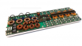
The optimization results reveal the asymmetrical flyback (Figure 2) as the best-suited topology among the considered candidates for highly compact chargers since it offers the highest efficiency.
The asymmetric flyback topology features ZVS of the primary half-bridge by utilizing the magnetizing current and ZCS of the synchronous rectification switch and lays the foundation for the highest conversion efficiency. The converter is operated with a fixed turn-ON time of the low-side switch of the primary half-bridge, which is determined by the resonance frequency and varying turn-ON time of the high-side switch, which depends on the input voltage. This results in a varying switching frequency. Because this converter operates in mixed flyback/forward mode, it will be called hybrid flyback from now onwards.
Figure 2 shows the realized demonstrator. The adapter is designed to deliver an output power of 65 W with a peak power capability of 105 W for several milliseconds. The converter is USB-PD compliant; it is designed for an input voltage range from 90VAC to 264VAC and delivers output voltages from 5VDC to 20VDC. Depending on the input voltage, the demonstrator operates from 100kHz to 200kHz. The conducted EMI requirements according to FCC Part 15 Class B and EN 55022 Class B are being fulfilled with a 6 dB margin.
The converter efficiency reaches 93.8 percent under worst-case conditions and a peak efficiency of 95 percent. The uncased power density is around 27 W/in³. In reality, the power density of the cased converter will not be higher than 22 W/in³ to avoid a thermal runaway.
For an optimum operation over input voltage, output voltage and output load the converter operates in a multimode operation which keeps the efficiency as high as possible from low-load to full-load. Infineon´s XDP™ digital controller family embeds a microprocessor core surrounded by all digital and analog circuits needed to realize a power supply with only a few external components. The controller can be configured by the user in a very flexible way allowing optimization for different application use cases.


Figure 2: Hybrid flyback converter
Influence of the Adapter Dimensions
Power density and converter efficiency are closely linked together. A thermal simulation helped to examine the influence of the housing size and the usage profile.
For simplification, the converter was modeled and simulated as a solid copper block with certain power dissipation. Figure 3 shows the used model. As output power again 65 W was chosen, and the maximum allowed case temperature was limited to 70 °C. 1.5 mm thick Plexiglas was used as casing material, and cooling was ensured via heat transfer and heat radiation. It was also assumed that the wall plug has very low heat conduction and heat radiation.

Figure 3: The simulation model
In the first step, the influence of the position of the adapter was evaluated. A 65W adapter with a density of 15 W/in³ was used as a basis for the simulation. However, the results, shown in figure 4, are also valid for other power densities.
It was found, that the highest amount of heat can be removed by plugging the adapter directly into a wall plug (position 3d). The worst case is given if the adapter is positioned on a desk according to position 1a. Position 3d allows removing around 20% more heat than position 1a.

Figure 4: Influence on the position of the adapter
In the next step, the influence of the case size was investigated. The dashed line in Figure 1 shows the relation between power density and converter efficiency. For the simulation, a cubical shape with a height of 19 mm was chosen because of a possible direct connection to a wall plug.
It is worth to mention that a thin and flat adapter case would not allow improving the power density. Especially in position 1a around half of the casing cannot contribute for removing the heat.
Requirements and Regulations
Figure 2 shows that the main transformer, electrolytic capacitors as well as EMI filter determine the size of the adapter. A further power density increase would only be achievable by a size reduction of these components.
One possibility is to increase the operating frequency. Theoretically, this allows reducing the size of the transformer as well as of the EMI filter. One of the key enabling technologies for doing so — GaN power switches — is available nowadays.
The theoretical reduction in the size of the transformer is caused by the fact that as an increase in frequency by e.g. a factor of 2 makes it possible to reduce the number of turns of the windings by a factor of 2 under the condition of a constant flux density and the same core geometry. This means less space for the winding is needed, and a smaller core could be used. However, core losses and also copper losses increase with the operating frequency. In order to avoid an unwanted efficiency decrease or to overheat the component, this may require to reduce the flux density and therefore to increase the number of turns again. The needed space for the windings increases and the transformer is becoming bigger again.
Besides this, there are requirements from the safety standards regarding creepage and clearance distances as well as the maximum operating temperature of the magnetic component, which also limits the possible size reduction. It is worth to mention, that a general safety regulation (EN 60664-4) is existing, which regulates the creepage distance depending on the operating frequency. According to this regulation, the creepage distances more than double for operating frequencies above 800 kHz.
The size of the primary bulk capacitor is determined mainly by functional requirements, i.e., ripple voltage, minimum input voltage as well as output power. Increasing the operating frequency will not help. Here requirements and capacitor size need to be adjusted. Last but not least, an increase in the operating frequency may help to reduce the size of the EMI filter. During the filter design, parasitic effects just like stray inductances and magnetic couplings need to be taken into consideration as these could influence the functionality a lot.
USB-PD adapters are on the way to penetrate the market. New control methods, digital regulation schemes, and new highly efficient ZVS/ZCS topologies enhance the behavior of the good old flyback converter.
These new techniques allow us to increase the operating frequency and to shrink today’s bulky adapters by a factor of 2-3. The influence of the converter efficiency to the maximum possible size reduction of the converter under worst-case conditions needs to be considered. Otherwise, thermal runaway can happen.
Considering all the above-described influences, the design of a reliable product with power densities of more than 20W/in³ is feasible, which allows using the same adapter for notebooks, tablets, and mobile phones and other devices.
About the Authors
Dr. Manfred Schlenk is an Experienced Senior Principal Power Systems with a demonstrated history of working in the semiconductors industry. Strong information technology professional skilled in Application-Specific Integrated Circuits (ASIC), Product Development, Semiconductors, Engineering, and Cross-functional Team Leadership.
Alfredo Medina-Garcia received his Master of Science in Telecommunication Engineering, then he worked as an electronic engineer at SMPS innovation Infineon Technologies.
Christian Wald worked at Infineon that is a world leader in semiconductor solutions that make life easier, safer and greener. Microelectronics from Infineon is the key to a better future. In the 2019 fiscal year (ending 30 September), the Company reported sales of €8.0 billion with about 41,400 employees worldwide. Infineon is listed on the Frankfurt Stock Exchange and in the USA on the over-the-counter market OTCQX International Premier.
References
- Panepinto, P.A. Making power adapters smarter and greener. In Proceedings of the 2009 IEEE International Symposium on Sustainable Systems and Technology, Phoenix, AZ, USA, 18–20 May 2009; pp. 1–5.
- Steigerwald, R.L.; de Doncker, R.W.; Kheraluwala, M.H. A comparison of high power DC-to-DC soft-switched converter topologies. In Proceedings of the 1994 IEEE Industry Applications Society Annual Meeting, Denver, CO, USA, 2–6 October 1994; Volume 2, pp. 1090–1096.
- Deboy, G.; Kasper, M.J.; Medina-Garcia, A.; Schlenk, A. A New Era in Power Electronics with Gallium Nitride. ETG J. Infineon Article 2018, 2, 6.
- Medina-Garcia, A.; Kasper, M.J.; Schlenk, M.; Deboy, G. Asymmetrical flyback converter in high-density SMPS. In Proceedings of the PCIM 2018, Nuremberg, Germany, 5–7 June 2018.
- Huber, L.; Jovanovic, M.M. Analysis, Design and Performance Evaluation of Asymmetrical Half-Bridge Flyback Converter for Universal-Line Voltage-Range Applications. In Proceedings of the Applied Power Electronics Conference and Exposition (APEC 2017), Tampa, FL, USA, 26–30 March 2017.
- Medina-Garcia, A.; Schlenk, M.; Morales, D.P.; Rodriguez, N. Resonant Hybrid Flyback, a New Topology for High-Density Power Adaptors. Electronics 2018, 7, 363.
This article originally appeared in the Bodo’s Power Systems magazine.