Facebook
 Google
 GitHub
 Linkedin
Getting GaN Right: Solving the Materials Challenge
GaN is in high demand for AI, EVs, and more high-power needs, but engineers must overcome challenges in materials technology and supply chain.
GaN is having its moment—and rightly so. The material offers fast switching, lower energy loss, and solid thermal performance. It supports the kinds of high-efficiency, high-density power systems we’re building today for AI infrastructure, EV platforms, renewables, and industrial controls. But if you’re an engineer trying to put GaN into production, you know the performance gains aren’t free. They’re set at the materials level—not the device—which means they come with a set of real, persistent materials challenges.

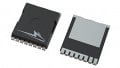
GaN wafer.
Growing GaN
The first thing to know is that GaN doesn’t want to be grown on silicon. The lattice constants and thermal expansion coefficients don’t match. When you force them together, nature pushes
back. You get stress. You get dislocations. You get defects. And unless you solve for those things early—right at the epitaxial level—you can’t build a reliable device.
That’s where I spend most of my time. My background is in epitaxy, and I’ve spent more than two decades working on compound semiconductors. For GaN, I’ve always said the device begins at the atomic level. If the materials stack is wrong, nothing downstream will behave the way you want it to.
One of the most overlooked parts of the process is growth initiation. That’s where a lot can go wrong fast. If you don’t get the interface clean and stable from the first nanometer, you’ll end up with parasitics and performance loss that can’t be fixed later. In RF, you’ll see degraded signal integrity. In power, you’ll see inconsistent switching behavior and thermal drift. The device might still work—but not predictably, and not at the efficiency levels we’re targeting.
In the past, engineers tried to sidestep this by either keeping GaN applications in low-voltage, low-power spaces or shifting to silicon carbide. SiC gives you better lattice matching, but it’s expensive and limits wafer size. That doesn’t help if you’re trying to hit cost and scale targets for automotive, compute, or infrastructure markets.
GaN on Silicon
GaN on silicon is the path forward—but only if the epitaxy holds up. At IQE, we’ve spent the last decade working on exactly that. We’ve built epitaxial platforms for GaN on 150 mm and 200 mm silicon wafers that deliver good morphology, low defectivity, and tight uniformity across the wafer. It didn’t happen overnight. We’ve had to rethink buffer layer design, implement better stress compensation, and refine every step of the growth process. But it’s working.
What we’re seeing now is GaN-on-silicon that performs well in high-voltage environments, supports MHz-range switching, and integrates cleanly into system-level designs without blowing up your thermal budget. That unlocks real flexibility for power architects. You can shrink the magnetics. You can drop the heat sink size. You can push power density without compromising efficiency.
That’s starting to show up in commercial systems—in rack-level converters for AI compute, onboard EV chargers, and solar inverters. These aren’t lab demos. These are real deployments, and they’re only possible because the material stack is finally doing what it’s supposed to do.

GaN wafers
But I’ll be clear—just getting the materials right isn’t enough. While GaN-on-Si epiwafers are designed to be compatible with standard CMOS production lines—allowing manufacturers to leverage existing fab infrastructure—the reality is still nuanced. The epitaxy remains specialized, and the process windows are tighter than what legacy silicon typically demands. So even with CMOS-compatible processing, trying to do it all in-house using a conventional vertical integration model can mean spending a lot of time and capital solving problems that others have already streamlined.
That’s why we’ve leaned into what we call virtual vertical integration. We work closely with foundries, device designers, and OEMs to stay aligned on specs, reliability, and production targets. Our job is to deliver high-quality materials that match what downstream needs, not to build the whole stack ourselves. That kind of focused collaboration gets GaN into systems faster, with fewer process surprises and lower integration risk.
One area where this model is especially relevant is AI infrastructure. Everyone’s talking about GPUs and compute throughput. Fewer people are talking about what’s happening at the power level. These systems are drawing more energy, and without higher-efficiency power conversion, the infrastructure becomes the bottleneck.

GaN on silicon
GaN enables higher switching speeds with lower losses. That means you can reduce conversion stages, tighten packaging, and improve rack utilization. I’ve seen customers shave significant power overhead just by rethinking their front-end power architecture with GaN. It’s not incremental—it’s enabling.
And it’s not just about performance. It’s about scale. Data centers can’t keep growing if the power budget keeps climbing. You have to address that at the materials level. GaN helps get you there.
The Supply Chain
There’s also a broader strategic point to consider. With all the current focus on domestic semiconductor capacity, GaN stands out. It’s not as locked in globally as logic or memory. That means there’s still room for leadership. But you can’t lead if you don’t control the materials. You need epitaxy capability, processing expertise, and a qualified supply chain to support it.
We’re supporting that development in Europe and the U.S., and we’re working with partners across sectors—compute, automotive, aerospace—to make sure the GaN ecosystem is ready. The interest is there. What’s needed now is consistency, predictability, and the confidence to design it in at scale.
If there’s one thing I’ve learned working with compound semiconductors, it’s that the materials either make your job easier—or make it impossible. With GaN, we’ve reached the point where the performance is proven. The next step is reliability. And that starts at the atomic level.