Facebook
 Google
 GitHub
 Linkedin
High Performance Flybuck
This article discusses the different methods that can be used to improve the performance of a Flybuck converter in a wide input voltage or power level range.
A Flybuck is an alternative to a Flyback for low power applications because it is a low-cost, simple to use an isolated topology. Just synchronous buck and coupled inductor windings are needed to create isolated outputs. Furthermore, a Flybuck typically achieves softer switching compared to a Flyback topology. This can eliminate the need for a snubber circuit and lowers Electromagnetic Interference (EMI).
Improve the Performance of Flybuck
But how can we improve the performance of a simple Flybuck further? This article presents three different methods, which can be used individually or simultaneously. First, using an inverting topology will influence the duty cycle range and therefore will improve performance and efficiency in many applications. Second, adding a synchronous rectifier will reduce the secondary side losses and will improve the output voltage regulation. The last method will improve the output voltage regulation further by adding an optocoupler to regulate the output voltage.
Figure 1 shows a simplified schematic of an inverting Flybuck with the optocoupler and secondary synchronous rectification.
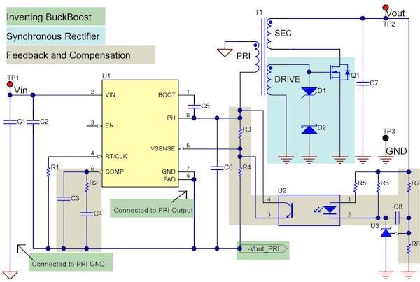
Figure 1: Simplified schematic of a high-performance Flybuck
In a Flybuck, the minimum input voltage must always be higher than the primary output voltage. Very often this results in a high duty cycle for a low input voltage. That is a disadvantage in many Flybuck applications because high duty cycles will increase peak currents a lot. Therefore with large amounts of leakage inductance, the Flybuck is probably not usable with a duty cycle higher than 60%.
Fortunately, there is another alternative. An inverting BuckBoost can be used instead of a Buck since this will lead to a lower duty cycle in many applications. Of course, it is only attainable if a positive voltage on the primary side is not needed because the BuckBoost is generating a negative primary voltage.
Every synchronous Buck controller can be used for realizing an inverting BuckBoost that generates a negative output voltage. It is just a simple trick needed to get the controller working. In a standard Buck, the output voltage is connected to the inductor and the return line is connected to GND. For an Inverting BuckBoost, simply connect the device ground to the negative output (instead of to GND) and connect an additional capacitor between the input and the negative output. (see Figure 1). In this configuration, the Buck controller will generate a negative output voltage. Care must be taken about the maximum VDD voltage rating of the controller. After the output is in regulation, the controller is referenced to the negative output. Therefore, the maximum VDD voltage seen by the controller is the voltage difference between the input and the output voltage. Please note that the UVLO will not work properly because it is much lower in this configuration.
Secondary Side Synchronous Rectifier
There are different methods to drive secondary side synchronous rectifiers. You can add a separate Gate drive transformer to drive the secondary synchronous FET. If a primary controller is used with external primary MOSFETs then the driving signal could be taken from the primary side.
Another method is to use a secondary-side synchronous controller, which is expensive but typically leads to perfect control of the FET. A simpler and cheaper way than both these methods is to add a gate drive winding to the Flybuck transformer. This “self-driven” technique only costs a few cents, but unfortunately, this simple method has a drawback. The timing cannot be controlled perfectly which may result in a short shoot-through current. This will increase the power dissipation and reduce efficiency. The circuit should be verified in the lab to ensure safe operation under all conditions. Nevertheless, a self-driven synchronous rectifier will improve the efficiency and the output voltage regulation compared to an output diode. Figure 1 shows the simple circuit of a self-driven synchronous FET (highlighted in brown).
Optocoupler Feedback
In primary side control, the secondary output voltage is regulated through the coupling of the primary side voltage. The secondary output is controlled only by the primary output and the transformer. Voltage drops of the output rectifier or parasitic elements like leakage inductance, a resistance of the windings, layout or other components cannot be compensated. Therefore, typically only an output voltage regulation of about 5% to 10% can be achieved. When better regulation is needed, an optocoupler can be used for regulating the secondary output voltage.
How does the regulation of the output voltage work?
Figure 1 shows the simplified circuit of an optocoupler regulated design. An error amplifier (U3) such as the TL431 is used together with an optocoupler to provide feedback loop isolation. A small variation of the output voltage due to the line or load changes is sensed by the input of the error amplifier and compared to an internal voltage reference. Differences between the divided down output voltage (R7, R8) and the voltage reference are converted into an error current.
This error current signal is transferred to the primary side through the optocoupler. On the primary side, the controller (U1) is regulating the negative primary voltage. Similar to the secondary side, a resistor divider (R3, R4) is used to measure and compare the output voltage with the internal voltage reference of the controller. In other words, there are two feedback paths, one on the primary side and one on the secondary side. Combining these two feedback paths is simply done by connecting the Opto-transistor to the primary side resistor divider (see Figure 1).
The Opto-transistor is in parallel to the high side resistor (R3), therefore, the effective resistance can only be decreased. For this reason, the primary side resistor divider must be chosen carefully. In order that the secondary loop can control both directions (increasing and decreasing the output voltage) the primary loop itself must regulate a higher primary voltage (absolute value) than required. This means that the primary side voltage divider must be set for a higher absolute value of the negative output voltage. Therefore, the secondary loop has the ability to increase and decrease the output voltage which is needed during transients.
A Rising Popularity
The Flybuck topology is particularly prevalent in applications with a wide input voltage range or a wide power level range, the performance of a Flybuck is sometimes not sufficient. The presented methods showed ways to improve the behavior of this isolated topology.
A practical example of an inverting Flybuck with optocoupler feedback and synchronous rectification is shown in the PMP30197 reference design from Texas Instruments. The peak efficiency is above 92% (see Figure 2) and the load regulation is better than 1.5%. All technical documents such as Schematic, Test report, BOM or Gerber Files can be downloaded here.
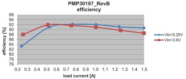
Figure 2: Efficiency Reference Design PMP30197
About the Author
Florian Mueller was born in Rosenheim, Germany, in 1976. He received his degree in electrical engineering from the University of Haag. After working for several years as a freelancer in the field of electrical engineering, he joined TI in 2011 and is working in the European Power Design Services Group, based in Freising, Germany. His design activity includes isolated and non-isolated DC/DC and AC/DC converters for all application segments.
References
- Texas Instruments' Powerlab reference design library with more than 1500 fully tested power reference designs.
- Reference Design PMP30197
- Power Supply Technologies and Controllers