Facebook
 Google
 GitHub
 Linkedin
Biricha Lecture Notes on Analog and Digital Power Supply Design Part 2B
This article highlights Biricha Digital Power Ltd voltage mode compensator design for all hard switched Forward type non-isolated voltage mode converters.
In the previous article, we discussed power supply compensators in detail; we can now design our first compensator to stabilize a voltage mode, Forward type power stage. But first let us have a quick word about voltage mode control.
Voltage mode is one of the earliest forms of switch mode power supply control and its operation is very simple. The design method presented here can be applied to all hard-switched “non-isolated” Forward type converters with or without a transformer (i.e. Buck, Forward, Push-Pull, Half-Bridge, Full Bridge). We will discuss current mode control and opto-isolated power supply design in great detail in future articles.
All we have to do is to look at the output voltage; if it goes up with respect to the desired value, we reduce the PWM duty and if it goes down we increase it. As such, all we are doing is regulating the output voltage with respect to our desired “reference” voltage.
Of course, the manner with which we change this duty is dictated by the compensator that we design i.e. the position of its poles and zeros. The compensator should give us good transient performance, whilst at the same time make sure that we do not violate the stability criteria.
Voltage Mode Compensator Design
For voltage mode control we almost always need a Type III compensator. The circuit for our Type III compensators is given in figure 1.
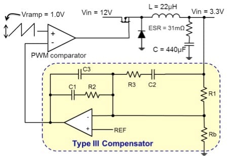
Figure 1: Type III compensator
From previous articles we know the transfer function Hc(s) and equations relating the poles and zeros to component values:
Please note that these are in radians per second but we usually work in Hz so please don’t forget that 2π scaling factor.
Here wp0, wp2 and wp3 are the compensator’s poles and wz1 and wz2 are its zeros. Of course Biricha Digital’s automated power supply design software (Biricha WDS) automatically designs highly optimised compensators as discussed in the previous articles. However, if your transient response requirements are not very stringent, you can easily design a stable compensator by hand for most Buck/non-isolated Forward topologies.
Consider a Buck converter shown in figure 1. We can see all the necessary values from this figure. Below is a step-by-step guidelines how to quickly design the compensator for this converter:
Step 1: Determine plant Bode plot
Setting the transformer turns ratio to 1:1 for now, for all Forward type topologies in voltage mode the plant bode plot is very simple; of course a Buck converter can be represented as a Forward converter with a transformer turns ratio of 1:1 at 1/(2π √LC).
Ignoring the PWM block for now, typically we have a resonant bump and an Equivalent Series Resistance (ESR) zero at 1/(2π ESR C). Using the values of L, C and ESR shown in figure 1, we can easily calculate the positions of the resonant bump and the ESR zero of the plant bode plot as shown on figure 2.
From this figure, you will notice that unlike a standard LC filter, our low-frequency gain is not 0 dB. This is the impact of our PWM comparator and in many textbooks that is called the “PWM Gain”. Again for voltage mode Buck converters this is very easy to calculate and is equal to our input voltage divided by the PWM ramp voltage of our controller IC, (i.e. Vramp in figure 1).
We know our input voltage (12V in our case) and the PWM ramp voltage is always specified in the datasheet of our IC (for simplicity we have taken this to be 1V). In our case, therefore, the low frequency gain will be 20.Log(12V/1V) = 21.58dB.
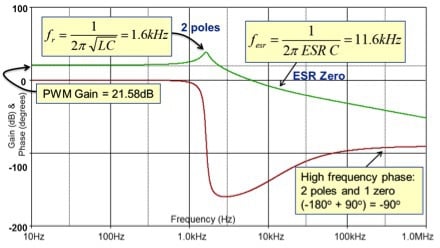
Figure 2: Plant Bode plot
Finally if we have a transformer in our circuit, all we need to do is to scale the gain plot by the transformer turns ratio. This completes the Bode plot of our plant and we can now design the compensator.
Step 2: Calculate Compensator pole/zero locations
The method presented here is an easy approximation to allow you to quickly calculate these for a compensator with relatively good performance with reasonable crossover frequencies. There are of course more accurate methods, and there are good books which have detailed analysis (please see the bibliography) but first and foremost, credit should be given to Dean Venable for his pioneering work in this field. Our WDS software uses exact equations to allows the user to specify exact phase margin and crossover frequency; but for now all we need is a hand calculator and piece of paper
You can see from the compensator’s transfer function that we have 2 pole, 2 zeros and 1 pole at origin. To get reasonable performance:
- Place 2 compensator zeros right on top of the plant’s double poles (i.e. at 1.6kHz),
- Place 1 compensator pole at ESR zero to cancel the plant’s zero (i.e. at 11.6kHz),
- Place the other compensator pole at half the switching frequency (i.e. if we have a switching frequency of 200kHz we place this pole at 100kHz). This will help in reducing high frequency noise,
- Finally we place the pole at origin at:
Where Fx is the desired crossover frequency. In our case let us design for Fx = 10kHz and therefore we will have to place our pole at origin at 833 Hz (i.e. 1V×10kHz/12V).
Step 3: Calculate compensator component values
Now that we know the positions of our compensator poles and zeros, we can use the equations above to calculate component values in a step-by-step manner:
- Start calculating R1 and Rb base on the current pass through and the reference voltage need on the controller IC. Then, check to make sure that the power dissipation per resistor does not exceed ~60mW so that it doesn't get a hotspot on PCB. Do not let the current fall below 100µA for robustness in the EMC test chamber during the susceptibility test. R1 and Rb form a potential divider (or sampling divider) and this sets the demand reference voltage (in our case let us assume that this is 2.55V). So we know the input voltage of the potential divider (in our case this is Vout = 3.3V) and we know the output voltage of the potential divider fed to the IC (in our case 2.55V). Starting by allowing 1mA of current through this pot and using the standard potential divider equations and Ohms law we have: R1 = 750Ω, Rb = 2.55kΩ, and power dissipation in each resistor < 60mW.
- By having R1, the equation for wp0 can be used to calculate C1 (please don’t forget that these equations are all in rad/sec so we need to scale by 2π. Furthermore, C1 is usually much larger than C3 and therefore the equation for wp0 simplifies to wp0 = 1/ (R1×C1).
- By having R1 and wp0 can calculate C1 (in our case C1 = 1 / (2π×833 Hz×750Ω) = 250nF.
- Equation for wz1 is dependent on C1 and R2. We now know wz1 and C1 so we can calculate R2 = 390Ω.
- Again as C1>> C3 equation for wp2 simplifies to wp2 = 1/ (R2 C3). This pole is being placed on our ESR zero (i.e. @11.6kHz) and we know all the terms apart from C3 so we can calculate it. C3 = 34nF.
- Finally, we are left with the equations for wp3 and wz2. These two are dependent on each other but we have 2 equations and 2 unknowns, therefore we can easily solve them. If we divide the equation for wp3 by the equation for wz2, then oth C terms and the 2π terms cancel and we are left with all the known variables and we can solve for R3:
With R3 calculated (in our case R3 = 12Ω) we can substitute back into equation for wp3 and hence calculate our very last component: C2 = 130nF.
We can easily use WDS in “manual pole/zero placement” mode to verify our calculations. WDS provides us with all the important stability parameters as well the Bode plot. WDS Bode plot for our design is shown in figure 3 and the stability information is shown in figure 4.
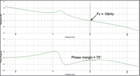
Figure 3 – Simulated loop bode from Biricha WDS
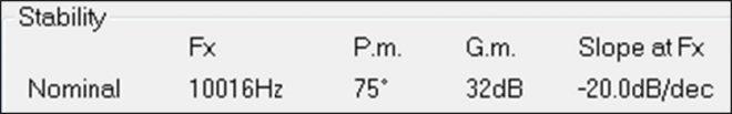
Figure 4 – Stability data from WDS for our design
From figures 3 and 4, we can see that we have achieved a crossover frequency of 10kHz as desired and a phase margin of 75 degree. Slope at crossover is -20db/decade and our gain margin is better than 32dB. Thus, we have designed a very stable power supply with a respectable crossover frequency and even though we had no control over the phase margin, 75 degrees is more than ample.
Voltage Mode Compensator Design with Plants Containing a Transformer
If our Forward type topology has a transformer but no isolation, (e.g. does not have an optocoupler) then the design procedure is exactly the same as above with just one minor difference. All we have to do is to multiply our pole at origin by the turns ratio of the transformer.
For example if we had a Forward converter with exactly the same specification as the Buck converter in this article, but with a transformer turns ratio of 10:1, then all we would have to do is multiply our pole at origin by 10 (833 Hz × 10 = 8330Hz). The rest of the calculation and procedures will stay exactly the same.
Concluding Remarks
In this article, we discussed how to design a compensator for all hard switched Forward type non-isolated voltage mode converters. An approximate method has been presented that will give reasonable results in most cases.
The advantage of the method presented here is that it is very easy and quick to calculate but we do not have any control over the phase margin. We also included a complete numerical example down to component value selection.
In the forthcoming articles we will discuss current mode control, isolation and why generally it is not a good idea to use a PID controller to stabilise a voltage mode power supply.
About the Author
Ali Shirsavar holds a Doctorate of Philosophy (PhD) in Power Electronics at the University of Reading, Berkshire, England. He is an Associate Professor at the University of Reading for more than 17 years then became the Director at Biricha Digital Power.
References
- Biricha’s “Analog Power Supply Design Workshop” Manual
- Switching Power Supplies A – Z by Sanjay Maniktala, ISBN: 978-0123865335
- Switch-Mode Power Supplies, Second Edition: SPICE Simulations and Practical Designs by Christophe Basso, ISBN 978-0071823463
Related Content