Facebook
 Google
 GitHub
 Linkedin
Predicting The Load Transient Response of Switch Mode Power Supplies
This article offers a method to predict the load transient response to have the optimal combination of the output filter and the loop compensation network.
This article shows a method to accurately predict the load transient response. Therefore the optimal combination of the output filter and the loop compensation network can be figured out. It results in maximum performance and cost reduction.
Switch Mode Power Supplies (SMPS) must have a small transient deviation to a step change of the load current. The rate of change of the output voltage depends on the output filter and the bandwidth of the system. The minimum needed output capacitance is often miscalculated. If too much capacitance is used the overall cost increases and if too little is used the performance is insufficient. In this article, a method is described to predict the over- or undershoot of the output voltage due to a load transient. The method can be used for calculating the minimum needed output capacitance that must be added to meet the specifications of the design.
Control Loop
A lot of papers describe the compensation techniques. Fortunately, the method to get a stable system is almost independent of the topology. The output filter, consisting of the output inductor and the output capacitor, must be compensated. The output filter behaves like a 2nd order system if the controller works in voltage and in Continuous Conduction Mode (CCM). Things change for current mode control or Discontinuous Conduction Mode (DCM). The current mode controller controls the inductor current. The inductance acts as a current source and the second order system degenerates to a first order system. Just the output capacitor and the load resistance remain as an output filter. Typically a Type II (for current mode) or Type III (for voltage mode) compensation network is used to generate a stable system. The total open-loop is the sum of the power stage loop and the compensation loop. The total open-loop defines first of all the stability of the system. Well-known stability criteria such as a gain margin of more than 10dB and a phase margin of more than 45° must be fulfilled. The total open-loop can be measured with a frequency response analyzer as shown in picture 1 which includes the bode plot of the power stage, the compensation, and the total open-loop. The total open-loop has a second very important function. It has the ability to reduce the output impedance and therefore improving the performance. What variable dictates the load transient response? It is simple, the output impedance of the closed-loop. It is the output impedance reduced by the total open-loop.
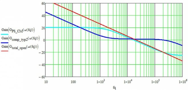
Figure 1: Bode plot: Powerstage, Compensation and total open loop turquoise: Powerstage; blue: Compensation; red: total open loop
A Different View of the Total Open-Loop
Any periodic continuous-time waveform can be represented by a summation of sinusoidal waveforms (harmonics) with different amplitudes and frequencies. A Fourier series expansion applied to the output voltage results in a very good approximation of the system behavior. The total open-loop of the system describes the ability to filter the harmonics up to the crossover frequency. Any output voltage change due to a load step leads to a response of the loop. The output voltage over- or undershoot can be represented as the sum of the harmonics. The loop filters these harmonics up to the bandwidth (= crossover frequency fco) if the phase margin is high enough. Therefore only harmonics with a higher frequency than fco remain. The summation of the remaining harmonics results in the output voltage load step response. That is the reason that the closed-loop output impedance at fco dictates the load transient response.
In other words, the total open-loop reduces the output impedance up to the bandwidth if the phase margin is high enough. That is usually the case because the phase margin must be greater than 45° for stability reasons. If the phase margin is 60° then the impedance of the open-loop is equal to the impedance of the closed-loop at fco. For predicting the load step response the output impedance at fco is crucial.
Current Mode Control
In current mode control, the output inductor behaves as a constant current source feeding the output filter capacitor. The output filter behavior is 1st order, defined by the output capacitor.
The impedance of the output capacitor is simple the series circuit of the capacitance, the ESR (equivalent series resistance) and the ESL (equivalent series inductance).
ZCout(s)=1s⋅Cout+ESRCout+s⋅ESLCoutZCout(s)=1s⋅Cout+ESRCout+s⋅ESLCout
Figure 2 shows the open-loop impedance (turquoise) of the output capacitor. Open-loop means that there is no feedback, the system is unregulated. The main point of interest is what happens if the system is regulated due to negative feedback. What changes the impedance for a closed-loop system? What does it mean to close the loop?
The transfer function of the power stage and the Type II compensation network build the total open-loop of the system. In a closed-loop system, the total open-loop lowers the output impedance up to fco. The closed-loop output impedance is equal to the open-loop output impedance divided by one plus the total open-loop gain.
Zout,open(s)= the open-loop impedance
G→total,open(s) = open-loop of the system
Figure 2 shows the effect of closing the loop graphically.
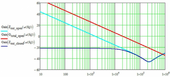
Figure 2: total open loop, open loop impedance, closed loop impedance. turquoise: open loop impedance; red: total open loop; blue: closed loop impedance
Again, for predicting the load transient response the closed-loop output impedance at the bandwidth (=fco) is needed.
Therefore following formula predicts the load transient response very accurately.
Cout,min,CMCout,min,CMis the minimum output capacitance needed to keep the voltage ripple less thanΔVtransientΔVtransient for a loadstepΔIloadstepΔIloadstep.
This formula can be simplified if ceramic capacitors with very low ESR are used and the phase margin is 60 degrees. (If the phase margin is 60° then the open-loop output impedance is equal to the closed-loop impedance at fco)
The simple formula for current mode is:
Voltage Mode Control
The approach for voltage mode control is the same as for current mode control. The output impedance depends on the inductor and the capacitor:
The derivation for the minimum needed output capacitor for voltage mode (second order system) leads to the following equation:
![C_{out\_min\_VM} = \frac{1}{2 \pi \cdot bandwidth} \cdot \frac{1}{\left [ \frac{1}{\frac{\Delta I_{loadstep}}{phasemargin\_factor \cdot \Delta V_{transient}} - \left [ \frac{1}{(DCR\_L_{out} +2 \pi bandwidth \cdot L_{out})} \right ] } - ESR_{Cout}\right ]}}](https://eepower.com/uploads/thumbnails/ql_c0d42bac8310b2bddbe65041c8860899_l3.png)
Getting Accurate Load Transient Response Results
Using the derived equations leads to very accurate results. The minimum needed output capacitance to fulfill the specification can be calculated very fast and exactly. The development time and the cost of the design will be reduced. Texas Instruments provides a library with almost 2000 tested TI Designs. There are many designs calculated with this method, like some buck controller (e.g. TPS54xxx series) or flyback quasi-resonant controller (e.g. LM5023, UCC28600). Please visit www.ti.com/powerlab.
About the Author
Florian Mueller was born in Rosenheim, Germany, in 1976. He received his degree in electrical engineering from the University of Haag. After working for several years as a freelancer in the field of electrical engineering, he joined TI in 2011 and is working in the European Power Design Services Group, based in Freising, Germany. His design activity includes isolated and non-isolated DC/DC and AC/DC converters for all application segments.
References
- Vatche Vorperian, “Fast analytical techniques for Electrical Circuits”
- J. Betten, R. Kollman, “Easy Calculation Yields Load Transient Response”
- A. I. Pressman, “Switching Power Supply Design”