Facebook
 Google
 GitHub
 Linkedin
Biricha Lecture Notes on Analog and Digital Power Supply Design Part 2A
This article discusses commonly used compensators in power supplies and explains their circuits, transfer functions, and their poles and zeros.
In the previous articles we covered all the basic foundation material needed to understand the fundamentals of power supply compensator design. In this article we will discuss commonly used compensators in power supplies. We will explain their circuits, transfer functions and their poles and zeros.
In the majority of the cases, analog compensators for PSUs, take the form of an inverting op-amp which is usually internal to the controller IC, plus some external capacitors and resistors. Of course the capacitors and resistors determine the position of the poles and zeros based on the transfer function of the op-amp circuit. Building on the material covered in the previous articles, we are now in an ideal position to cover this topic.
One thing to remember about PSU compensators is that there is nothing scary about them. We are simply dealing with an inverting op-amp with some impedances, just like what we studied in our very first few lectures at university.
Consider the generic inverting op-amp in Figure 1
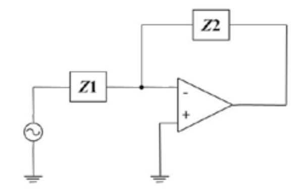
Figure 1 – Generic inverting op-amp
We know from university lectures that the transfer function of this circuit is:
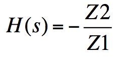
Where Z1 and Z2 are usually a combination of capacitors and resistors. With this simple circuit we can construct almost all of the compensators that are used in analog power supplies.
Type I Compensator
If I now replace Z2 with a capacitor (C = 10nF) and Z1 with a resistor, (R = 1.6kΩ) I will have created myself a simple Type I compensator. Furthermore, by selecting the values of the capacitor and the resistor I can control the position of any poles and zeros that this compensator has. Please note that for simplicity of teaching we are not considering the dc reference source usually connected to the non-inverting input and the biasing resistor usually connected between the inverting input and ground. These two elements only affect the dc analysis and do not impact the ac transfer function of our compensator; in other words they have no impact on the position of our poles and zeros.
My transfer function therefore becomes:
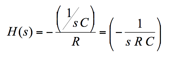
My gain at a certain frequency f will be:
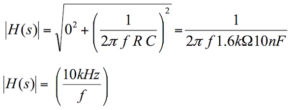
And taking into account the inverting action of the op-amp, the phase f will be:
Looking at the above equations there some very important observations to point out:
We have a pole at the origin as the denominator of the transfer function becomes zero only when s = 0.
From the gain equation, we can see that the gain at low frequencies approaches infinity. This in general is exactly what we want in a power supply, as a high gain at low frequencies translates into near zero steady state error.
Again from the gain equation we can see that the gain becomes 1 at f = 1/ (2 p R C), i.e. when f = 10kHz. This means that in dB world the gain plot crosses the zero dB axis. Many textbooks or application note call this “the position of the pole at origin”. What they actually mean is “the frequency at which the gain due to the pole at origin will cross the 0 dB point”.
This is the terminology that we will use from now on. Hence, from now on, every time we say “we place the pole at origin at a certain frequency,” we mean that we select the values of resistors and capacitors such that the gain plot due to the pole at origin crosses 0 dB at a certain frequency.
From the phase equation we can see that we have a phase lag of -90°. Which of course is the characteristics of having single pole in our system.
Type I compensators are relatively rare in high performance power supplies and we have it included here for teaching purposes and to explain the concept of the position of the pole at origin. Type II and Type III compensators are by far more common and the vast majority. Let us go through them.
Type II Compensator
This is one of the most popular compensators as it is almost always used in current mode power supplies. We will discuss current mode control in a later article.
The circuit, including a simple buck power stage is given in figure 2.
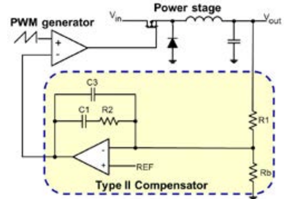
Figure 2 – Type II compensator circuit. Please note that the PWM generator and the op-amp are usually internal to our IC
The transfer function is for this compensator is:
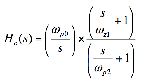
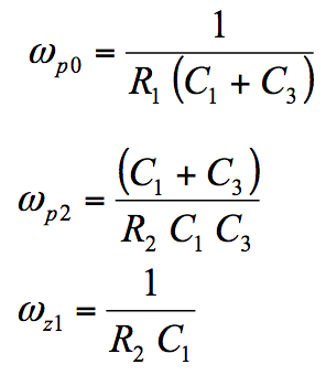
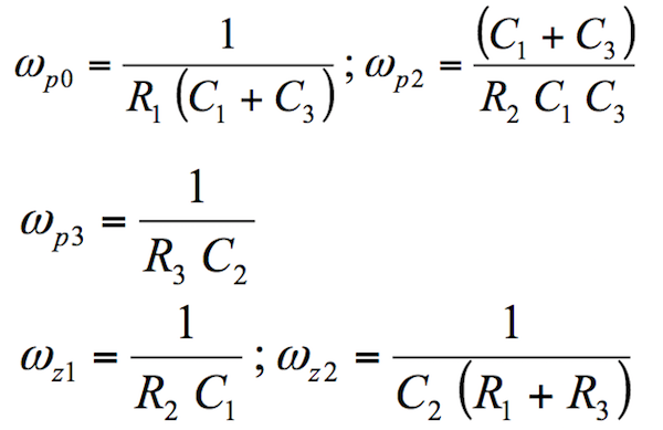
Referring back to our previous lecture notes, we can immediately identify that we have 1 pole at origin (wp0), a second pole (wp2) and a zero (wz1). Please note that the equations are in rad/s and as always the component values determine the position of these poles and zeros:
It is easy to see that by appropriate selection of the component values we can place our poles and zeros in such a way to shape our Bode plots so that we meet the stability criteria as discussed in earlier articles.
You can see from the transfer function that we have one zero. This of course means that we can force a maximum phase boost of 90°. But sometimes 90° of phase boost is just not enough; a case point being almost all our voltage mode power supplies. We therefore need another compensator that allows more phase boost; this is our Type III.
Type III Compensator
The circuit for our Type III compensators is given in figure 3
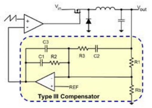
Figure 3 – Type III compensator
With an addition of just an extra resistor and capacitor (R3 and C2) we can convert our Type II compensator into a type III and get the extra phase boost that we need. The transfer function is given below:
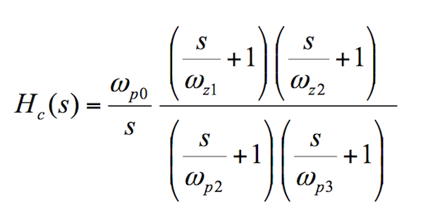
We can see now that again we have our desirable pole at origin to remove our steady state offset, but this time we have an extra pole (wp3) and more importantly and extra zero (wz2) compared to our Type II compensator. The presence of 2 zeros of course suggest that we can have 180° of phase boost compared to our Type II’s 90°.
The equations determining the positions of our poles and zeros are:
How Well Does the Transfer Function Match with Reality
The good news is that with just these two transfer functions we can pretty much stabilise most of the analog power supplies in the world. We will learn how to place the poles and zeros and step-by-step real life design in future articles. For now let us experiment with the values of resistors and capacitors to place our poles and zeros and then measure a real compensator to see if it matches with our theory.
We will use Biricha Digital’s automated power supply design software to first design a Type III compensator, then we will build and measure with a Bode 100 network analyser. You can see from figure 4 that Biricha WDS has placed the poles and zeros of the compensator and calculated the component values. The nearest preferred values of the components are given in the right hand column of figure 4.
Inserting the component values in the equations of the Type III compensator above should give exactly the same poles and zeros as calculated by WDS and shown in the figure. Please note that the equations given earlier are in rad/s, but in WDS they are in Hz. For now we are not interested in the pole zero placement strategy; we will discuss detailed design in a later article. For now we are just making sure that our equations are correct and the simulated frequency response fits well with the real life one.

Figure 4 - Component values and the simulated poles and zeros of a type III compensator as calculated by WDS.
The comparison between the simulated Bode plot and the real measurement of a real compensator with the component values of figure 4 is shown in figure 5. You can see that we have almost a perfect match and therefore our equations are correct and the component values accurately place the poles and zeros of the compensator exactly where we expect them to be.
All we need to do now is to devise a strategy for placing our poles and zeros such we meet our specifications and the stability criteria. We will do this, in detail in the next few articles.
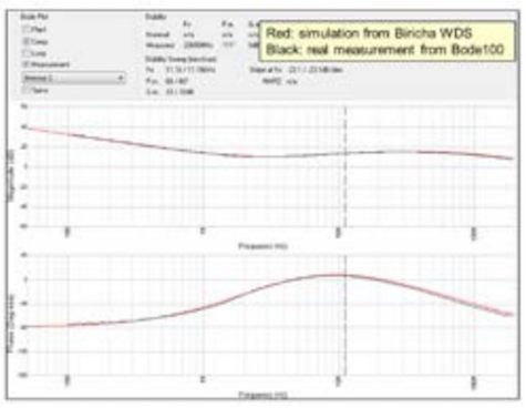
Figure 5 – Type III compensator Bode plot simulated by Biricha WDS vs. real measurement
Concluding Remarks
In this article, we discussed compensators, their poles and zeros, transfer functions and clarified what we mean by the phrase “placing the pole at origin at a certain frequency”. We showed, once again, that our mathematical presentations of our circuits match almost perfectly with real measurements. Furthermore, we detailed all the necessary equations relating the values of capacitors and resistors to the position of our compensators’ poles and zeros.
We are now ready to start designing our compensators to stabilise our power supplies. In the next few articles we will discuss voltage mode and current mode control strategies and go through the compensator design procedures in a step-by-step manner.
About the Author
Ali Shirsavar holds a Doctorate of Philosophy (Ph.D.) in Power Electronics at the University of Reading, Berkshire, England. He was an Associate Professor at the University of Reading for more than 17 years. He then became the Director of Biricha Digital Power.
Bibliography
- Biricha Digital’s Analog Power Supply Design Workshop Manual
- OMICRON Lab website For the PDF version and related videos.
This article originally appeared in the Bodo’s Power Systems magazine.
Related Content