Facebook
 Google
 GitHub
 Linkedin
GaN ePower Ultrafast Switches With Integrated Gate Drivers
This article provides an example of the benefits of integrated GaN power ICs via the introduction of an integrated FET and gate driver IC.
Gallium nitride FETs have continued to gain traction in many power electronic applications, but GaN technology is still in the early part of its life cycle [1]. While there is much room to improve basic FET performance figures of merit an even more promising avenue is the development of GaN power ICs.
The lateral FET structure of modern GaN-on-silicon devices lends itself to the monolithic integration of both power and signal devices, and integrated GaN power ICs are beginning to appear commercially [2], [3]. This integration promises to reduce size and cost while simultaneously improving reliability and performance.
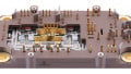
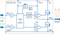
This article provides an example of the benefits via the introduction of an integrated FET and gate driver IC. This IC was conceived primarily as a laser driver for indirect time-of-flight applications and is capable of driving 10 A pulse currents from a 40 V bus. The output rise and fall times of this IC are under 600 ps while switching 10 A, it has an output RDS(on) of approximately 50 mΩ. and can switch at over 100 MHz. This IC is part of a family of components that can accommodate different supply and logic family inputs. All current members of this family have the same 2×3 BGA chip-scale package (see figure 1) with a 1 mm × 1.5 mm footprint. This package has excellent thermal performance and extremely low inductance.

Figure 1: Photo of the IC (a) and block diagram (b) for EPC21601 fully integrated GaN power switch.
Laser Driver Requirements
Laser drivers for lidar are pulsed power applications. Figure 2 shows a simplified laser driver. Initially, switch Q1 is off and C1 is charged to the input voltage VIN. A command signal command causes switch Q1 to discharge C1 fully, or partially, through laser diode D1. Inductor L1 represents the stray inductance of the C1D1Q1 loop. Modern lidar systems demand high current and narrow pulses with short transitions. In simple terms, the faster the driver, the better the resolution; and the higher the current, the further the range. Depending on the lidar system, pulses may range in width from 1 ns to 100 ns, and from 1 A to more than 100 A.

Figure 2: Simplified schematic of the laser driver
Two major forms of lidar dominate the lidar industry today: direct time-of-flight (DTOF) and indirect time-of-flight (ITOF) [4]. Typical DTOF lidar sends individual pulses and times the reflection to compute the distance to the target. ITOF lidar works by comparing the phase of a transmitted and reflected pulse train. ITOF lidar has recently shown tremendous growth due to the ability to use simplified receivers and therefore achieve lower cost. Imaging chips have been developed based on low-cost CMOS camera imaging technology that lets the imaging chip provide distance information for each pixel. This is turn allows an entire frame of distance information to be captured at once. These are sometimes referred to as “flash lidars” since they use the laser as a flash lamp to illuminate the scene. Though initial designs have been done with silicon laser drivers, these have short-range and suffer from poor image quality as well as lower frame rates due to the weak and poorly shaped laser pulses. GaN FETs have proven effective in these designs by enabling higher currents and faster pulses with sharper edges in a cost-effective manner.
Typical ITOF Specs for Portable Lidar Systems
Much of the growth in ITOF lidar has been in the medium range, from less than 1 meter to 10s of meters. These systems range from single-point distance measurement systems to megapixel TOF cameras, but the trend skews towards multi-spot and imaging systems due to the ability to capture a wide field of view in one detection cycle. This trend favors a light source that can illuminate the entire scene at one time and this is a natural fit for vertical-cavity surface-emitting lasers (VCSELs).
Individual VCSELs are very small, but since they emit from the die surface, many VCSELs can be integrated on a single die to increase the light output. For small, portable systems, typical pulse current requirements range from 2-10 A. While the voltage drop of a single VCSEL is small at low currents, the equivalent series resistance can cause a substantial voltage drop at higher currents. A series connection of VCSELs can further increase voltage drop. Wire bonds, which are often used to connect to the VCSEL, can contribute additional voltage drop due to the added inductance. Today, the voltage drop of the VCSEL can range from 3 V to 30 V, with many applications needing ≥ 10 V. When operating in burst mode, the pulse frequency may range from a few MHz to beyond 100 MHz.

Figure 3: ITOF operation overview diagram.
Since ITOF imagers use phase difference detection, the shape of the waveform is important. The use of rectangular pulses greatly simplifies phase detection and has the added benefit of using a switch as the modulator. This simplifies the laser driver and greatly reduces total system power requirements. To summarize, a laser driver for an ITOF lidar system should be capable of generating 2 to 10 A pulses from a bus as high as 30V, with switching frequencies ≥ 100 MHz possible, and minimum pulse widths of 2 ns or less. This is a wide range of specifications and the usual approach has been a custom GaN-based laser driver design for each application. With silicon-based laser drivers, much of this design space is completely out of reach.
Benefits of ntegration
Modern eGaN® power FETs with the required current and voltage ratings have rise and fall times of less than 1 ns and can therefore easily meet the above requirements. In fact, a single 0.81 mm2 eGaN FET, like the automotive qualified EPC2203, can meet the entire design space above. However, the drive requirements for such FETs are not directly compatible with the outputs of the digital subsystem generating the transmit pulses, since these tend to be low voltage logic of 3.3 V or less and have low drive current capability. Hence, a gate drive is required to interface the digital signal to the FET. This is a problem since there are very few gate drivers capable of driving eGaN FETs up to 100 MHz and beyond while maintaining fast rise and fall times. The few that have the required drive capability consume unacceptable levels of power. Furthermore, the physical distance between the gate drive and FET adds inductance to the gate loop, further decreasing performance. Finally, the gate driver takes space (more space than the FET), adds cost and reduces reliability. GaN technology enables the integration of the gate drive with the main FET, thus improving performance, reducing part count, and capturing all the attendant benefits.
Performance
Efficient Power Conversion has developed a family of monolithic GaN IC laser drivers, as shown in Figure 1. Key preliminary specifications for the primary version are shown in Table I.
| Parameter | Condition | Minimum | Nominal | Maximum |
| VD | 40V | |||
| ID | 10A | |||
| VDD | 5V | 5.5V | ||
| VDD | 1.6V | |||
| VIL | 0.8V | |||
| Pulse Width | 10A, 20V | 2ns | ||
| Propagation Delay | 10A, 20V | 3ns | ||
| Max Switching Frequency |
10A, 20V | 100MHz | ||
| Transition Time | 10A, 20V | 600ps | ||
| RON | 41mΩ | 54mΩ | ||
| IDD | 5A, 20V, 30MHz |
50mA |
Table I: Key specifications of the EPC21601 laser driver at 25°C.
There are three members of the IC family: (1) 2.5 V logic input with a 5V supply to the IC, (2) 5 V logic input and a 12 V supply, and (3) low-voltage differential signaling (LVDS) input enabling it to be driven directly from high-speed digital ICs in a noisy digital environment. All three variations are available on the same 2×3 BGA chip-scale package with a 1 mm × 1.5 mm footprint and require only a single bypass capacitor.
Figure 4 shows some typical waveforms driving a 2 Ω low inductance load in place of the laser. With a supply voltage of 20 V, the resulting current pulses have an amplitude of 10 A. Figure (4a) shows a single pulse. The drain voltage vdrain fall time t f measures the turn-on time, and tr the turn-off time. At the maximum rated current, tf = 602 ps and tr = 306 ps. Lidar transmitters often use burst mode, with one reason being the need to prevent laser overheating. Figure (4b) shows a 100 MHz burst of 10 cycles. The IC can operate at 100 MHz and 10A continuously but burst mode operation is to prevent the load power dissipation from excessive heating.

Figure 4: Single pulse waveform (a) and 100 MHz burst waveform (b). Both cases use 2.5 V logic level input and 20V supply with 2 Ω load. Yellow trace is input (1 V/div) and red trace is drain voltage (5 V/div or 2.5 A/div)
Figure 5 shows some typical waveforms driving a vertical cavity surface emitting laser (VCSEL). Figure (5a) shows a single pulse and Figure (5b) shows a 100 MHz burst of 10 cycles. The VCSEL packaging includes a bond wire that adds considerable inductance, which results in drain waveform ringing and a slower optical output risetime. Note that the higher impedance due to this inductance and the 10 V transition result in a turn on time (fall time tf) of less than 300 ps.

Figure 5: Waveforms driving a vertical cavity surface emitting laser (VCSEL). Single pulse waveform (a) and 100 MHz burst waveform (b). Both cases use 2.5 V logic level input and 10V supply with a VCSEL load. Yellow trace is input (1 V/div), red trace is drain voltage (5 V/div) and blue trace is optical receiver output (5 mV/div).
What’s Next?
There are several other potential applications for the newly developed IC. A more traditional power electronics use would be a tiny boost converter for circuits that have only a 5 V supply and which need an additional higher voltage. In fact, such a converter would be very useful to develop the laser driver bus voltage in a lidar application. Another potential application would be a small Class E or EFn inverter [5], [6], or converter for tiny wireless power sources. There are many possibilities and with a 40 V, 10 A logic-controlled power switch capable of 100 MHz switching, the door to new applications and ideas is wide open.
About the Author
John Glaser holds a Ph.D. and a Master's Degree in Electrical and Computer Engineering at the University of Arizona and a Bachelor's Degree in Electrical and Computer Engineering at the University of Illinois at Urbana-Champaign. He has achieved 11 patents and 2 publications throughout his career and specializes in high-frequency power conversion, VHF power, wide bandgap (WBG) gallium nitride (GaN) and silicon carbide (SiC) power semiconductor applications, high-density power conversion, power RF circuits and applications. He currently works as the Director of Applications Engineering at EPC since June 2014.
References
- A. Lidow, M. de Rooij, J. Strydom, D. Reusch, and J. Glaser, GaN Transistors for Efficient Power Conversion, 3rd ed. Wiley, 2019.
- Efficient Power Conversion Corporation, “EPC2152 Datasheet, Rev. 1.3.” Jul. 20, 2020, Accessed: Oct. 03, 2020. [Online]. Available: https://epc-co.com/epc/Portals/0/epc/documents/datasheets/ EPC2152_datasheet.pdf
- D. Kinzer and S. Oliver, “Monolithic HV GaN power ICs: Performance and application,” IEEE Power Electron. Mag., vol. 3, no. 3, pp. 14–21, Sep. 2016, doi: 10.1109/MPEL.2016.2585474.
- C. Bruschini, P. Padmanabhan, and E. Charbon, “LiDAR Fundamentals,” presented at the SENSE Detector School, Schloss Ringberg, Jun. 20, 2019, [Online]. Available: https://www.sensepro.org/images/OutreachEducation/EPFL_LIDAR_SENSEworkshop_Jun2019_v3.pdf
- Andrei Grebennikov and Nathan O. Sokal, Switchmode RF Power Amplifiers, 1st ed. Elsevier, Inc., 2007. [6] S. Kee, “The Class E/F Family of Harmonic-tuned Switching Power Amplifiers,” Ph.D., California Institute of Technology, 2002.
This article originally appeared in the Bodo’s Power Systems magazine.
Related Content