Facebook
 Google
 GitHub
 Linkedin
Automotive PCB Properties and Design Considerations
Electronic elements have been playing an increasingly active role in automotives. At present, a top-level vehicle possibly contains more than 200 electronic
Electronic elements have been playing an increasingly active role in automotives. At present, a top-level vehicle possibly contains more than 200 electronic control units some of which are sensors and processors applied in car cockpit. It can be concluded that the value of electronic products serving for automotives lies in dynamical system, body and chassis and the majority of them are concerned with digital power.
Application of electronic systems in automotives aims to increase auto performance, covering three aspects: environmental improvement, security enhancement and convenience and comfort.
- Environment improvement refers to fuel saving, tail gas reduction, fuel transformation from gasoline, natural gas, bio-fuel to hybrid power and pure power. Electric vehicles, thus, have become a strategic direction for the automotive industry.
- Security enhancement lies in traffic accident reduction, ranging from airbag, radar monitoring, stereo camera, infrared monitoring and automatic avoidance to autonomous driving. Currently, autonomous vehicles are attracting majority attention and invest from the globe.
- Convenience and comfort is generally rooted in audio, video display, air-conditioner, computer, mobile communication, internet, navigation and electronic toll collection for considerations of convenience and humanization.
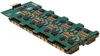
As the backbone of electronic devices, PCBs (Printed Circuit Boards) applied for automotives have to meet the requirement listed above as well.
Fundamental Requirement for Automotive PCBs
Quality Assurance Requirement
A basic demand of long-term quality assurance for manufacturers or distributors lies in a sound quality management system, that is, ISO9001 from an international perspective. Owing to the particularity of automotive industry, three leading automotive manufacturers from North America co-established a quality management system in 1994 uniquely for the automotive industry, that is, QS9000. At the beginning of the 21st century, a new quality administration system was published by world automotive manufacturers based on regulations of ISO9001, that is, ISO/TS16949.
As technical regulations for automotive industry around the globe, ISO/TS16949 integrates special requirement for automotive industry and focuses on defects prevention, quality fluctuation and waste reduction in the supply chain of automotive components.
Therefore, the first certificate automotive PCB manufacturers have to achieve is ISO/TS16949 prior to their genuine entry into the auto market.
Basic Requirement on Performance
High reliability
Automotive reliability mainly comes in two aspects: one hand is service life during which control units and electronic components are able to normally work whereas the other hand is environmental resistance which allows automotive control units and electronic components to excellently behave in extreme environment.
The average service life of automotives is from 10 to 12 years during which only components or vulnerable parts can be replaced. In other words, electronic system and PCBs have to feature such service year as that of automotives.
Vehicles tend to be affected by climate and environment in the process of application, ranging from freezing cold, extreme heat and long-term shining and rain. Apart from those, they have to suffer from environmental changes led by heat generated due to working electronic components and systems. So do automotive electronic systems and PCBs. Automotive electronic systems have to defeat the following harshness in the environment including temperature, humidity, rain, acrid smoke, vibration, electromagnetic interference (EMI) and current surge.
Light weight and miniaturization
Light weight and miniaturization are beneficial to fuel saving, which results from light weight and miniaturization of each component and circuit board. For example, the area of automotive-applied ECU (Electronic Control Unit) was 1,200cm3 at the beginning of the 21st century while that has been shrunk by four times at least. Light weight and miniaturization of PCBs derive from density improvement, area reduction, thinness and multiple layers.
Performance Properties of Automotive PCBs
Multiple Types
As combinations of mechanical and electronic devices, modern vehicle technologies integrate both ancient and traditional techniques and up-to-date scientific technologies. Different parts in modern vehicles depend on electronic devices with different functions, leading to applications of PCBs with different missions.
Based on distinction in terms of substrate material of PCBs for automotives, they can be classified into two categories: inorganic ceramic-based PCBs and organic resin-based PCBs. The leading property of ceramic-based PCBs is high heat resistance and excellent dimensional stability, applicable for engine system in highly-thermal environment. Nevertheless, ceramic-based PCBs feature bad manufacturability, leading to a high cost of circuit boards. With the development of newly-developed resin substrate with increased heat resistance, resin-based PCBs are mostly applied in the majority of modern vehicles.
One general rule is followed: PCBs using substrate materials with different performances are applied in different sections of a vehicle, responsible for the implementation of different functions. The following table demonstrates PCB type compatible with part of vehicle devices or instrument.
| Vehicle Devices | PCB Types |
| Speedometer; air conditioner | Single/double-layer PCB Single/double-layer flexible PCB |
| Car stereo; monitor | Double-layer PCB Multi-layer PCB Flexible PCB |
| Automotive communication devices; wireless location appliances; security control system |
Multi-layer PCB HDI PCB Flexible PCB |
| Engine system; power transmission control system | Metal-core PCB Rigid-flex PCB |
| Vehicle power controller; navigation device | Embedded PCB |
Reliability Requirement on PCBs at Different Sections of Vehicles
As a type of transportation tool concerning public security, automotives belong to a range of products with high reliability. Apart from ordinary dimensions, appearance and performance requirement on mechanics and electronics, a series of tests concerning reliability have to be implemented on them.
Thermal Cycling Test (TCT)
Five levels are set in accordance with different sections of a vehicle. Thermal cycling temperature for PCBs located at different sections of a vehicle can be summarized in Table 2 below.
| Vehicle Section | Level | Low Temperature | High Temperature |
| Within vehicle body | A | -40°C | 85°C |
| Vehicle chassis below | B | -40°C | 125°C |
| Above engine | C | -40°C | 145°C |
| Transmission parts | D | -40°C | 155°C |
| Within engine | E | -40°C | 165°C |
Thermal Shock Test (TST)
It’s quite normal that automotive PCBs are applied in extreme heat environment, which is especially challenging for heavy copper PCBs since they have to suffer from both external heat and heat resulting from their own bodies. Thus, higher requirement is called for heat resistance of automotive PCBs.
To take part in thermal shock test, automotive PCBs have to be immersed in solder paste with a high temperature of 260°C or 288°C for 10 seconds three times, after which qualified PCBs feature no issues such as lamination, bumps or copper crack. Nowadays, lead-free soldering has been used in PCB assembly with a relatively high soldering temperature, which adds more necessity to thermal shock test.
Temperature-Humidity Bias (THB)
Test Automotive PCBs have to go through numerous and dynamic surroundings including rainy days and humid environment, which makes it necessary to carry out THB test that is also capable of inspecting PCB CAF (Conductive Anodic Filament) mobility. CAF just occurs in the following situations: between adjacent vias on circuit board, adjacent vias and wires, adjacent wires and adjacent layers. Insulativity in those situations decreases or even leads to shortcuts. Insulation resistance should be determined by distance between vias, wires and layers.
Manufacturing Features of Automotive PCBs
High-frequency PCBs
Similar with military radar, as near-field radar, automotive anti-collision or predictive emergency braking system depends on PCBs to transmit microwave high-frequency signals. Thus, substrate materials with low dielectric loss are suggested, with PTFE (polytetrafluoroethylene) normally applied. Different from ordinary FR-4 as substrate materials, PTFE or similar high-frequency materials calls for distinct manufacturability naturally. For example, special drilling speed is required in the process of via drilling.
Heavy copper PCBs
Vehicles tend to generate more heat due to their high electronic density and power. With the number of hybrid power and all-electric vehicles rising, more advancing power transmission systems are demanded, which also calls for more electronic functions. It thus means higher demand for heat dissipation capability and larger current. To achieve that, the thickness of copper in PCB should be increased or copper leads and metal are embedded in multi-layer PCBs.
It’s easy to fabricate heavy copper double-layer PCBs while it’s quite difficult to fabricate heavy copper multi-layer PCBs. The key point lies in heavy copper graphics etching and heavy copper gap filling.
Inner circuit of heavy copper multi-layer PCBs is heavy copper. Afterwards, graphics transferring requires heavy film with extremely high corrosion resistance. Etching time should be long enough and etching device and technical condition should stay in an optimal state in order to ensure excellent circuits of heavy copper.
Because there’s a huge difference between inner conductor and insulator substrate material surface and ordinary multi-layer PCB stack up fails to make resin fully filled in, causing the generation of cavities, thin prepreg is then suggested containing a high amount of resin. Some multi-layer PCBs contain inner circuit with different copper thickness so that different prepreg can be used for areas with large distinction and small distinction.
Component embedment
Embedded component PCBs were first applied in cell phones to increase assembly density and reduce the product’s overall size, which is essentially important for other electronic products as well. That’s why embedment technology is used in automotive electronic devices.
Based on component embedment methods, there’re many embedded PCB manufacturing options:
- Groove is milled first then SMDs are assembled through wave soldering or conductive paste.
- Thin-film SMDs are first assembled on inner circuits through wave soldering.
- Thick-film components are printed on the ceramic base.
- SMDs are assembled through wave soldering and then resin is used for packaging. This type of embedded PCBs is more compatible with the demands of vehicles such as heat resistance, humidity resistance and anti-shock, with high reliability.
HDI technology
Similar with smart phones or tablet computers in terms of functions of entertainment and communication, vehicles call for HDI PCBs as well. As a result, microvia drilling, electroplating and interconnection technologies have to be applied in automotive PCBs.
Automotive PCB Design Considerations
Inductor orientations
When two inductors (or even two PCB wires) come close to each other, inductance will be generated. Magnetic field created by current in one circuit (Circuit A) will afterwards cause drive of current in the other circuit (Circuit B). This process is similar with mutual effect between transformer primary and secondary collars. When two currents interact with each other through the magnetic field, generated voltage is determined by mutual inductance (LM):
In this formula, YB is the error voltage input to Circuit B while LA is the current through Circuit A. LM is quite sensitive to circuit spacing, inductance loop area and loop direction.
Therefore, an optimal method to arrange all inductors in a circuit can be achieved through compact circuit layout and coupling balance reduction.
Distribution of mutual inductance is related with inductance alignment. Therefore, direction modification of Circuit B makes its current loop parallel to magnetic lines of Circuit A. To achieve that, inductors should be vertically arranged, which is beneficial to mutual inductance reduction.
Inductor layout rules for automotive PCBs:
- Inductor space should be as large as possible;
- Inductor alignment should be set at right angles so that crosstalk between them will be minimized.
Lead coupling
Similar with inductor alignment affecting magnetic field coupling, if leads are close to each other, coupling will be affected as well and mutual inductance will be possibly generated. The leading issue in RF circuit lies in sensitive component layout such as input matching network, receiver’s resonant channel and emitter’s antenna matching network.
Return current path should be as close to the main current path as possible with radiation field minimized, which is beneficial to current loop area reduction. Optimal low impedance path is normally grounding area under leads, that is, loop area is effectively limited in the area with dielectric thickness times lead length. If grounding area is split, however, loop area will be enlarged. For leads going across the split area, return current will be forced to go across high impedance path, which greatly increases current loop area. This type of layout also makes circuit accessible to mutual inductance.
In a word, integrated grounding should be ensured under leads as much as possible since integrated mass area grounding is beneficial to circuit performance improvement.
Grounding thru-hole
The main issue RF circuit has to solve usually lies in bad characteristic impedance of circuits, including electronic components and interconnection. Copper layer with low thickness is equivalent to inductance wire. Moreover, distributed capacitance can be formed by the combination between a copper layer and adjacent leads. As leads go through thru holes, inductance and capacitance characteristics will be displayed as well.
Thru-hole capacitance mainly derives from capacitance between copper at thru-hole pad edge and bottom copper. Another element affecting thru-hole capacitance is the cylinder of metal thru holes. Parasitic capacitance affects little since it usually just leads to low signal edge of high-speed digital signals.
The largest effect of thru holes is corresponding parasitic inductance aroused by interconnection. Because the majority of metal thru holes feature the same dimension as that of integrated components in RF PCB design, a simple formula can be used to estimate the effect of thru hole.
In this formula, LVIA is the integrated inductance of thru holes; h refers to via height with inch as unit; d refers to via diameter with inch as unit.
As a result, circuit layout should conform to the following principles:
- Inductance module should be established for thru holes in sensitive area;
- Filter or matching network depends on independent thru holes;
- Thinner PCB copper will reduce the effect of thru hole parasitic inductance.
Grounding and filling
Grounding or power plane defines a public reference voltage that supplies power to all components in the system through a low impedance path. Based on that scheme, all the electric fields can be balanced with excellent shielding scheme generated.
Direct current always flows through a low impedance path. Similarly, high-frequency current is also a path flowing through the lowest impedance at the first minute. Therefore, for standard PCB leads above ground plane, return current tries to flow into the grounding area rightly under leads. Afterwards, split grounding area arouses all kinds of noises, which further increases crosstalk through magnetic field coupling or current accumulation. As a result, ground integrity should be ensured as much as possible, or return current will drive crosstalk.
In addition, filling ground, also called protective wire, is usually applied for design of circuits containing areas where continuous ground is difficult to be arranged or that requires shielding sensitive circuits. Grounding thru holes can be positioned at terminals of wires or along the wires to increase shielding effect. Protective wires can’t be mixed with leads designed to provide return current path, which will bring forward crosstalk.
When copper area isn’t connected to ground or connected to ground at one terminal, its validity will be decreased. In some cases, parasitic capacitance will be generated with ambient impedance changed or potential path formed between circuits, which, thus, lead to bad effect. Simply speaking, if copper has to be arranged on the board, the same electroplating thickness should be maintained.
In the end, grounding area near antenna has to be taken into consideration. Any monopole regards grounding area, routing and thru-hole as a section of system balance and non-ideal balanced routing will affect radiation efficiency and direction of antenna. Therefore, the grounding area mustn’t be directly placed right under the monopole antenna of a circuit board.
To sum up, the following design principles should be conformed to in terms of grounding and filling:
- Continuous grounding area with low impedance should be provided as much as possible;
- Two terminals of filling wires should be connected to the ground with thru-hole array applied;
- Copper-coated lines have to be connected to the ground near circuit around which copper coatings aren’t necessary. When it comes to circuit boards with multiple layers, a grounding thru-hole should be arranged as signal lines are transferred from one side to the other.
In conclusion, automotive PCB design rules can be summarized into the following table:
| Inductor layout | Inductor space should be as large as possible; Inductor alignment should be set as right angles; |
| Integrated grounding | Integrated grounding should be arranged under leads; |
| Through holes | Inductance module should be set for thru-holes in sensitive areas; Filter or matching network depends on independent thru-holes; Thinner PCB copper reduces the effect of thru-hole parasitic inductance; |
| Grounding and filling | Continuous grounding area with low impedance should be provided; Connect terminals of filling wires to the ground with thru-hole array applied; Copper-coated lines have to be connected to the ground; |
About the Author
Dora Yang is a technical engineer from PCBCart, a China-based full turnkey PCB assembly service provider, since 2010. She specializes in electronic design, PCB manufacturing, surface finish and substrate material. She obtained her Bachelor's degree from China University of Petroleum and a Master's from Zhejiang University.
This article originally appeared in the Bodo’s Power Systems magazine.