Facebook
 Google
 GitHub
 Linkedin
Automated Acoustic Inspection for IGBT Modules
This article discusses the non-destructive inspecting of IGBT modules for internal structural defects such as voids, non-bonds, delamination and cracks.
High-power IGBT modules have long needed a non-destructive method to inspect for internal structural defects such as voids, non-bonds, delaminations and cracks. The best time for such inspection is after assembly but before encapsulation, which prevents rework. X-ray won’t find all of these defects, but the ultrasound of acoustic micro imaging systems will.
Introduction
For a long while IGBT modules could not be inspected by acoustic systems, because of the water that couples the scanning ultrasonic transducer to the module. Module makers feared that even the slightest residue left after the water had evaporated could turn into leakage paths at the high power levels involved.
Two years ago Sonoscan solved this problem for laboratory acoustic systems by inverting the transducer and placing it underneath the IGBT module, where it can scan the bottom surface of the heat sink. Along with the transducer came an upward-pumping water jet to maintain a constant column of water between the transducer and the bottom surface of the heat sink just above it. The design of the system made it impossible for water to reach the exposed power die and circuitry at the top of the module.
System designers have now taken this concept to its logical next step by putting together the first automated acoustic system (patents pending) for inspecting IGBT modules. Like other acoustic microscopes designed for the production environment, this automated system can achieve higher throughput than a laboratory system because of superior handling of the parts - in this case, IGBT modules.

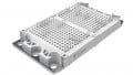
Figure 1: With doors open, the two IGBT modules are seen. The scanning transducers are out of sight beneath the modules.
The Difference from Laboratory Systems
Unlike laboratory systems, the automated system can be provided with automated loaders and unloaders to handle the IGBT modules. This means that it can be integrated directly into the production line. Modules to be inspected are stacked at one end of the system, which has two stages and two transducers to achieve higher overall throughput. In Figure 1 modules are masked to preserve the identity of the manufacturer. The transducers that one would expect to see just above the two PCBs are out of sight, one beneath each of the boards, and are upside down. Because the system is automated, the operator need only put the stack of modules to be inspected in place and activate the software recipe for inspecting this type of module. No human attention is needed from this point on.
An automated mechanical system loads two IGBT modules onto their respective stages and the scanning process begins. In some systems already in use, the only depth of interest in the modules is the solder layer binding the heat sink to the ceramic rafts above the heat sink. The targets here are voids, non-bonds, delaminations and cracks - important because these defects will block heat from reaching the heat sink and being dissipated from the module. The result could be overheating and failure of the module.
During scanning the transducer sends thousands of pulses of ultrasound per second through the water column and into the surface of the heat sink. Each of the thousands of x-y coordinates where ultrasound is pulsed each second will be represented in the acoustic image by a pixel whose color identifies the intensity of the echo. Ultrasound is reflected by material interfaces, and well-bonded interfaces between production materials typically reflect some portion of the pulse and transmit the rest across the interface. The reflected portion - the echo - is typically of moderate amplitude and will create a pixel that is some shade of gray. A material interface that is uniformly gray in an acoustic image is what an engineer typically wants to see.
What he does not want to see is a bright red feature, where the color red indicates that >99.99% of the ultrasonic pulse has been reflected as an echo. In a monochromatic acoustic image, these highest-amplitude echoes are bright white; they are often pseudocolored bright red (as here) for greater visibility. This type of echo is characteristic of the interface between a solid production material and a gas such as air, or a vacuum. The vast difference in material properties of air and, say, copper causes the essentially total reflection of ultrasound.

Figure 2: In this acoustic image, gray regions identify two ceramic rafts; red features in these regions are voids, non-bonds, delaminations or cracks in the solder layer.
This is what is seen in Figure 2, a segment of the acoustic image of a fairly large IGBT module. The gray square features are the acoustic image of the interface between the solder and two ceramic rafts below. The ultrasound was pulsed through the heat sink; heat sinks themselves are typically lacking internal features. The red features within the gray squares are areas where solder is either missing or not bonded to an adjacent surface.
The data that is collected during scanning is analyzed immediately. The system’s Digital Image Analysis™ (DIA) software will measure the total area of the voids in the solder above each ceramic raft. The accept/reject criteria, defined by the user, may call for a module to be rejected if the total area of voids is, for example, >2% of the area of the raft. Criteria may also take into account the x-y location of a defect - a void that is not directly under a die is not as serious as one that is. At the end of the scanning process, accept modules are stacked in front of the system, while rejects are stacked at the back. The acoustic data and images may be stored locally, in the system’s computer, or in the user’s Factory Information System.
The inspection process is thus carried out rapidly and with minimal human intervention. A technician will later examine the images of the reject modules to see which ones are candidates for rework, but no one needs to examine the images of the good modules.
The simplest inspection process, described above, is not the only alternative. In some instances, the inspection time can actually be reduced by using a recipe to scan only the significant regions of the module, and to skip the regions that do not have solder, die attach, or a die. This inspection process described to this point is suitable for inspecting a single layer of interest, such as the solder. But the user of the system may be concerned with defects at more than one level within the module. Typically the critical defects are voids in the solder layer and in the die attach material. Both can block heat and thus pose the risk of module failure.
Both the solder layer and the die attach layer can be imaged at the same time during scanning, without increasing the scan time. A scanning recipe is used that sets a gate for the solder layer - meaning that it accepts for imaging of the solder layer only those echoes whose arrival time indicates that they were reflected by a material interface between the heat sink and the raft. A second gate is set for the die attach material, which will use for imaging only those echoes that originated between the top of the raft and the bottom of the die.
The result of gating on two depths of interest is two acoustic images, one for the solder layer and one for the die attach layer. All that has changed is that software picks up two echoes from each pulse instead of one. The process takes no longer, and lets the user cover two potential trouble spots. Voids in the solder layer will be bright white. Voids in the die attach layer will also be bright white, but these echoes must travel through the solder layer on their way to the transducer. If there are voids in the solder layer, they will appear in the die attach image as black acoustic shadows because they blocked some of the ultrasound reflected from the die attach layer. It is possible, of course, that a void in the die attach layer will not be seen because a void in the solder lies directly between it and the transducer, but a module that has such a problem is very likely already a reject.

Figure 3: Made during the same scan as Figure 2, this image shows small red die attach voids at the largest of the three die.
The acoustic image in Figure 3 covers the same area as Figure 2, but was gated on the fifth of six depths within the IGBT module. The red defects seen in Figure 2 are here seen as black features because the ultrasound returning from the fifth depth is blocked by these voids. Thus the three-pronged void in the center of the left portion of Figure 2 is black in Figure 3. The depth that Figure 3 is gated on includes the interface between the ceramic raft and the die attach material. The small red features within the area of each die are voids in the die attach.
One benefit of gating, and especially of setting rather narrow gates, is that the tilting of ceramic rafts becomes more visible. If one region of a raft is actually displaying part of the solder layer, part of the die attach, then the raft is tilted and is a potential contributor to overheating.
Conclusions
What this new automated system provides is the ability to nondestructively inspect the internal features of IGBT modules at a high throughput rate according to the user’s definitions of accept and reject. Aside from startup, it operates without a technician to give the user higher module quality.
About the Author
Tom Adams is a consultant for Sonoscan, Inc., one of the most trusted authority on the application of Acoustic Micro Imaging (AMI) technology for nondestructive inspection and analysis. Sonoscan, Inc. is dedicated to technological innovation, and devotion to the highest quality results, and ongoing training and development.
This article originally appeared in the Bodo’s Power Systems magazine.