Facebook
 Google
 GitHub
 Linkedin
1500 V DC-Link Architecture is Essential to Solve the Need for More Power
Especially when renewable energies are used to supply the grid the use of power semiconductors becomes mandatory. One of the key questions in these applications from SSTs via ESS to MCS is how to achieve the best-possible efficiency. The solution: SiC modules and a DC busbar voltage of 1500 V.
This article is published by EEPower as part of an exclusive digital content partnership with Bodo’s Power Systems.
Recent years have seen technological advancements in key areas like solar photovoltaics (PV) and battery systems and the associated emergence of new technologies like solid state transformers (SST), energy storage systems (ESS) and megawatt charging systems (MCS). For power electronics, these advancements have increased focus on improving system efficiency, increasing the power density and reducing system costs.
In the case of solar PV systems, the continuous drop in photovoltaic module prices shifted the attention of developers towards lowering overall system costs. Initial efforts focusing on cost optimization of the individual components yielded minimal returns. For additional cost reduction, system level innovations were needed, and bus voltages were pushed higher to achieve lower currents at the same power levels. IEC and ANSI standards consider 1500 V to be in the low voltage category leading to the emergence of 1500 V bus voltage as the new baseline.
Adoption of higher bus voltages can also be seen in emerging megawatt charging systems where the charging connectors are designed to support 1500 V bus with a wide operating bus voltage maintaining backward compatibility to legacy power electronics [1].
To address the growing demand for 1500 V DC bus applications, Wolfspeed launched 2300 V WolfPACK™ power modules. The portfolio of 2300 V baseplate-less power modules utilize Wolfspeed’s 200 mm silicon carbide wafers and feature several improvements to maximize the 2300 V SiC MOSFETs inside. Aluminum Nitride (AlN) ceramic provides improved thermal performance with an increased thickness compared to standard Aluminum Oxide (Al2O3) ceramic increasing the case isolation voltage to heatsink. The module housing features a high CTI plastic material with a high comparative tracking index (CTI), reducing the creepage and clearance requirements for 1500 V bus applications.
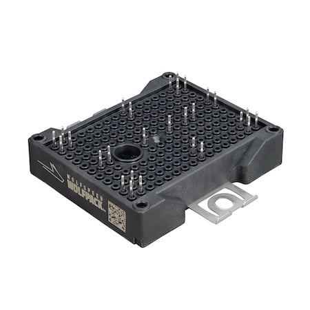
Figure 1. 2300 V Wolfpack GM module with high CTI plastic housing. Image used courtesy of Bodo’s Power Systems [PDF]
2300 V Technology Enhances System Durability
Durability is of paramount concern in applications demanding a 1500 V DC bus. This is particularly true in always-on applications like energy storage where the system bus voltage stays near 1500 V regardless of whether the system runs idle or at full load.
The cosmic ray FIT rate impacts MOSFET single event burn-out (SEB) events, which significantly impact device reliability. The failures-intime (FIT) of a device is defined as the number of failures expected in a billion hours of device operation and is specified in per unit area (FIT/ mm2) or per device. It is an indicator of the probability of random failures in power electronic devices installed in the field during the course its lifetime. Wolfspeed analyzed 2 kV and 2.3 kV device technology FIT rates at sea level to arrive at a strategic decision to adopt 2300 V to dramatically improve cosmic ray FIT over existing solutions on the market. At 1500 V bus voltage, there is an 8x improvement in FIT rate at 2300 V vs 2000 V SiC MOSFET technology, lowering the probability of a 2.3 kV SiC MOSFET to fail due to a single event burnout event by 8x than a similar 2 kV SiC MOSFET. (Figure 2)

Figure 2. FIT rate comparison of Wolfspeed 2.0 kV and 2.3 kV technology. Image used courtesy of Bodo’s Power Systems [PDF]
Voltage overshoots can be higher in 1500 V applications when a fast switching SiC device is used versus a similar system with silicon IGBTs. Equation (1) describes the voltage overshoot in a power electronic circuit with being the stray inductance of the power module and referring to the rate of rise of current.
\[\Delta V=-L_{STRAY}\cdot\frac{di}{dt}\,\,\,(1)\]
The voltage overshoot is high even for a few Nanohenrys (nH) of stray inductance due to the significantly higher values during the SiC MOSFETs switching. The additional 300 V margin (compared to 2000 V technology) enables faster switching without the lower breakdown voltage limit seen at 2000 V and reduces the turn-off requirements during overload conditions.
SiC-based Designs Improve System Performance Compared to IGBTs
2300 V technology enables realization of standard power electronic converter topologies at 1500 V bus with easy to implement 2-level topologies instead of complex 3-level topologies. For megawatt charging and energy storage applications, the trend is to push for higher switching frequencies. This is due to an increase in switching frequency improving the power density by a significant reduction in the size of passive filter components. At high switching frequencies, the total power semiconductor losses are expected to be dominated by switching losses. Hence, a comparison of switching losses will easily provide insights into the suitability of a device for this use case.
Figure 3 provides a total switching loss comparison between CAB7R5A23GM4 versus a 62 mm 1700 V IGBT half-bridge module at similar conditions. At a current of 200 A, 2300 V SiC MOSFETs offer 9x reduction in switching losses compared to the IGBT solution. This IGBT module was selected due to its form factor, similar current ratings and availability of switching data at a gate resistance of 1 Ω enabling a true comparison with a 2300 V GM Wolfpack. 1700 V IGBTs would not be selected for a 1500 V bus application, due to FIT rate and overshoot voltage concerns. A true 2000 V IGBT module of similar ratings will have far higher losses than seen in Figure 3 providing significantly better improvements.
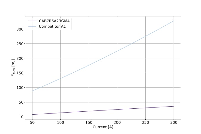
Figure 3. Switching loss comparison CAB7R5A23GM4 vs 62 mm 1700 V IGBT. Image used courtesy of Bodo’s Power Systems [PDF]
The alternative approach to realize a 1500 V bus system is the usage of 1200 V IGBT modules in a 3-level topology.
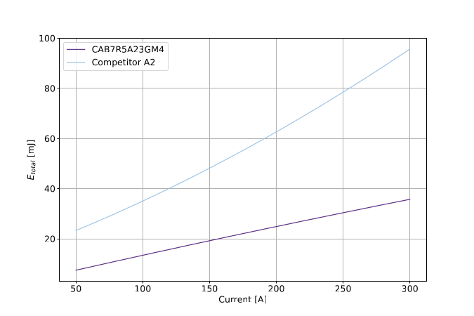
Figure 4. Switching data comparison of CAB7R5A23GM4 versus 1200 V 3-level IGBT module. Image used courtesy of Bodo’s Power Systems [PDF]
The switching loss comparison of a 1200 V IGBT module from competitor A in an equivalent package against CAB5R0A12GM4 is depicted in Figure 4 with similar operating conditions. The switching loss performance of SiC MOSFETs at 2300 V in a 2-level topology is still far more promising for high switching frequency applications.
System Simplification to Reduce System Cost
2300 V MOSFETs in 1500 V DC link applications enable a simplified 2-level topology and with higher switching frequency compared to silicon-based systems and significantly reduces the size of passives in the end converter application. This benefit can be observed by analyzing the power semiconductor selection from a system-level perspective when selecting semiconductors for a megawatt (MW) application. MW power levels are generally supported by 1200 V, 3-level IGBT modules in large 250 mm x 89 mm packages. A 1400 A power module can be replaced by 8 x CAB7RA23GM4 modules to deliver a MW of power. Figure 5 illustrates a switching loss comparison between CAB5R0A23M4 (scaled by 8) and a 1200 V, 1400A, 3-level IGBT module from competitor B.
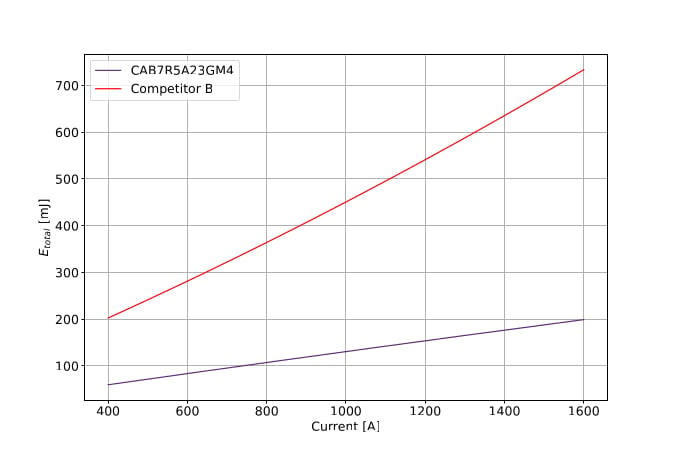
Figure 5. Comparison of switching losses for MW scale power applications. Image used courtesy of Bodo’s Power Systems [PDF]
Using 2300 V modules for a 1500 V megawatt level application includes additional advantages: WolfPACK modules enable a PCB power stage without specialized laminated busbar designs, thereby greatly reducing manufacturing complexity and final product costs. Furthermore, baseplateless 2300 V WolfPACK modules eliminate 1 layer in the thermal stack. Multiple WolfPACK modules (like 8 in the megawatt use case described above) help distribute the heat flux over a much wider area compared to the traditional bulky baseplate solution seen in IGBT modules at a significantly smaller footprint. The spread in heat flux also reduces the thermal cross coupling effects enabling better evacuation of heat generated by the modules. On top of this 2300 V enables a simplified 2-level topology at 1500 V versus the complex 3-level strategies seen with IGBTs. Consequently, capacitor voltage balancing requirement is eliminated. The availability of modules with pre-applied thermal interfaced material (PA-TIM) simplifies the mounting process to the heatsink and eases assembly workflow at manufacturing sites.
Conclusion
Energy generation, storage and consumption are in a time of unprecedented change as global focus on mitigating climate change grows. This family of 2300 V silicon carbide power modules helps to usher in a new way of designing solar, energy storage and megawatt fast charging systems to maximize system performance and reliability while reducing BoM, production, and maintenance costs. These first-of-a-kind power modules improve cosmic ray FIT by up to 8x over existing 2 kV solutions on the market and enable simplified 2-level system level architecture, meaning systems are less complex, experience improved uptime, and deliver unparalleled efficiency, ensuring a cleaner, brighter future.
[1] https://www.charin.global/media/pages/technology/knowledgebase/c708ba3361-1670238823/whitepaper_megawatt_charging_ system_1.0.pdf.
This article originally appeared in Bodo’s Power Systems [PDF] magazine.