Facebook
 Google
 GitHub
 Linkedin
SiC MOSFETs in Optimized Packaging Deliver a 3× Reduction in Switching Losses, Enabling Affordable High-Efficiency EV Battery Chargers
This article highlights Wolfspeed C3M™ SiC MOSFETs that considers package inductance and printed circuit board layout as factors for best system performance.
Advances in wide bandgap semiconductor designs are enabling SiC MOSFET die capable of increasingly faster switching speeds and lower switching losses. Improved low-inductance packages are essential in allowing circuit designers to take full advantage of this fast switching capability to improve power converter system efficiency and ultimately deliver energy savings to the customer.
Simple and practical improvements to commercially available discrete packages can significantly extend the performance of SiC MOSFETs without introducing proprietary packages that are difficult and costly to incorporate into a practical converter design.
This article describes the fundamental switching speed limitations of conventional discrete MOSFET packaging technology, presents and quantifies two new Wolfspeed packaging options, and shows how these new products can be used to cut losses and simplify the design of a 20kW active front end targeted for off-board, EV fast charging [1].
Introduction
With the introduction of Wolfspeed’s latest C3M silicon carbide MOSFETs, package inductance and printed circuit board layout are becoming critical factors in achieving the best system performance. C3M™ MOSFET die have been engineered to switch hundreds of volts and tens of amps per nanosecond. However, the large common source inductance of the conventional TO-247-3 package (due to source wirebonds and package source pin) causes a negative feedback mechanism that limits achievable di/dt and imposes associated switching losses.
As shown in the upper switch position of Figure 1, Q1’s source inductance (LS1) and corresponding voltage drop are shared by the power switching loop and the gate drive loop. During a fast di/dt switching transition, this common source voltage opposes the applied gate driver voltage (VDRV1). As a result, the gate-source voltage at the MOSFET die is reduced, significantly slowing switching transition speed and increasing switching losses. One solution to overcome this problem is to introduce new packaging options that include a dedicated Kelvin source pin to be used for the gate driver return connection, the KS pin shown in the lower switch position (Q2) of Figure 1.
When used with an isolated gate driver (VDRV2), the gate drive loop is no longer affected by the voltage appearing on the power switching loop source inductance. This breaks the negative feedback mechanism and enables significantly faster switching speed and lower switching losses.

Figure 1: Hypothetical MOSFET bridge leg with TO-247-3L upper device (Q1) and TO-247-4L lower device. The achievable di/dt in the TO-247-3L is limited because the voltage drop across common source inductance LS1 opposes the applied gate driver voltage VDRV1. The addition of a Kelvin source pin in the TO-247-4L combined with an isolated gate driver VDRV2 effectively removes this di/dt limitation, thereby drastically reducing switching losses.
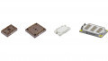
Wolfspeed has introduced two new SiC MOSFET package options with a dedicated Kelvin source pin; see Table 1 for the present product offerings. The first is a surface mount TO-263-7 package specifically designed for MOSFETs rated up to 1700V, while still having a 52 percent smaller footprint than D3PAKs commonly used for 1200 – 1700 V devices. Its five paralleled power source pins drastically reduce the power loop source inductance as compared to other surface mount packages. The second package option is a through-hole TO-247-4L featuring 8mm of creepage distance between the drain and source.

Table 1: Wolfspeed SiC MOSFET with Kelvin source pin
Measured Results: Validating Improved Switching Performance
The improved switching performance of the new package types has been validated using clamped inductive switching tests performed on the family of die products in Table 1. Figure 2 compares a 600V/ 40A turn-on switching transition for the 1000V, 65mΩ MOSFET die in a TO-263-7L package (with Kelvin source pin) vs. a TO-247-3L with no Kelvin source pin. Even for this moderately-sized MOSFET die with a conservative 10 Ω external gate resistor, the switching transition time is reduced from 72ns to 27ns resulting in a 2.6x faster transition.

Figure 2: Measured turn-ON switching transition for the same SiC MOSFET die product in two package options. The TO-263-7L package (using Kelvin source pin for gate return) switches 2.6x faster than the TO-247-3 (no KS pin).
Because this phenomenon is driven by MOSFET di/dt, the greatest opportunity for switching loss reduction is expected in the case of a large area MOSFET die switching high current levels and driven aggressively with low external gate resistance. A second clamped inductive switching test was performed using the 10mΩ, 900V die driven with VGS = -4 / +15 V, RG = 5 Ω, and VDD = 600 V. Figure 3 shows the switching loss vs. drain current when packaged in a standard TO-247-3L package (left) vs. TO-247-4L package with Kelvin source pin (right).
In both cases, the measured losses include the losses of the upper MOSFET’s intrinsic body diode being used as a freewheeling diode. The results demonstrate a potential 3.5× reduction in switching losses when measured near rated current.


Figure 3: Switching energy losses vs. drain current for the 10mΩ 900V SiC MOSFET in a TO-247-3L vs. TO-247-4L package. For this large area die driven with a 5Ω external gate resistor, a 3.5× switching loss reduction is observed near rated current.
Application: Cost-Optimized 20kW AFE for Fast Off-board EV Charger
The surge in demand for EVs has created new opportunities for SiC MOSFETs both on and off the vehicle. Half-bridge hard-switched circuits are used in drive-train DC/DC converters, traction drives, and PFC front end converters of battery chargers. SiC MOSFETs also enable higher frequency operation in soft-switched or resonant circuits commonly found in the DC/DC converter section of on-board and off-board DC fast chargers.
We have shown that these new packaging options and proper use of the Kelvin source pin offer dramatic reduction in switching losses for hard switching applications. Combining this switching performance with the 1000V C3M SiC MOSFETs’ low conduction losses over temperature, low QRR body diode, and more linear output capacitance allows circuit designers to breathe new life into a number of well-known, simple two-level circuit topologies. To demonstrate how these benefits can be monetized at the system level, Wolfspeed has developed and tested the 20kW two-level SiC-based active front end (AFE) shown in Figure 4, targeting the first stage of an off-board EV fast charger.


Figure 4: High-level technical specifications, 2L six-switch AFE power stage circuit topology, and realized 20kW AFE hardware prototype based on 2× C3M0065100K per switch position.
This two-level 20kW SiC-based AFE prototype is designed with 2× C3M0065100K MOSFETs per switch position with no additional anti-parallel freewheeling diodes. A switching frequency of 48 kHz has been selected to strike a good balance of phase-inductor cost-reduction, phase-current THD, and ease of EMI filter design (third harmonic below 150 kHz). Each phase inductance of 400 µH is constructed using a gapped AMCC 50 Metglass 2605SA1 core and copper foil windings.
A standard voltage-oriented control approach with space vector PWM is implemented digitally in a TMS320F28335-based control board. Dead-time has been reduced to ~100 ns in order to limit distortion near phase voltage crossings. The resulting measured efficiency and THD are shown in Figure 5, where all technical targets have been met.


Figure 5. Measured 2L SiC AFE efficiency and THD vs. power level (left) demonstrates that this simple topology and control approach can meet all targets. Measured efficiency and estimated power density for the 2L SiC AFE vs. several state-of-the-art published Si Vienna Rectifiers (right) demonstrates an approximate 1% improvement in efficiency via a 30% reduction in power losses.
Compared to the popular three-level silicon-based Vienna Rectifier topology, this approach offers a ≥ 30% reduction in power loss (kWh savings), circuit simplification, parts count reduction, easy control implementation, native support for bidirectional power flow (V2G), and similar net system BOM. Further details of the AFE prototype and comparisons to the Vienna Rectifier can be found in Reference 1.
Summary and Conclusion
The global market for power semiconductors deployed into cars is expected to grow by more than 3 billion dollars in the next five years due to increased electrification of vehicles [3]. Fast, highly-efficient on-board and off-board charging is becoming a key enabler to widespread adoption of EVs. Here, discrete SiC MOSFETs in intelligent economical packaging offer circuit designers new tools to improve power conversion efficiency, power density, and ultimately energy savings for the consumer.
An example two-level active front-end prototype has shown that Wolfspeed’s C3M SiC MOSFETs offer state-of-the-art system performance and a 30% reduction in power losses affordably while using a simple circuit topology and control approach.
About the Authors
Edgar Ayerbe is a senior marketing manager at Wolfspeed, a Cree company. He has a demonstrated ability of successfully introducing new disruptive technologies into the mainstream market. Skilled in new product definition, technical marketing, building an international customer base in Europe, China, Korea and Japan, Go-to-market Strategy, and Strategic Partnerships.
Dr. Adam Barkley is a SiC power device application engineer for power modules at Wolfspeed, a Cree company. Wolfspeed is a company that spent more than 28 years as part of Cree Inc., building the future with market-leading wide bandgap semiconductor products for the transportation, industrial, energy and communications markets.
Dr. John Mookken is a director on power applications at Wolfspeed, a company that spent more than 28 years as part of Cree Inc., building the future with market-leading wide bandgap semiconductor products for the transportation, industrial, energy and communications markets.
Reference
- A. Barkley, M. Schupbach, B. Agrawal, S. Allen, New 1000V SiC MOSFETs Enable Improved Efficiency, Density, and Cost Tradeoff Space for PFCs, Proceedings of the 32nd Applied Power Electronics Conference and Exposition (APEC 2017), Tampa, FL, USA, March 26-
- J. Mookken, Fast Charging EV with the Latest 1kV 3rd Generation SiC MOSFET. Proceedings of the 32nd Applied Power Electronics Conference and Exposition (APEC 2017), Tampa, FL, USA, March 26-30, 2017.
- IHS 2017
This article originally appeared in the Bodo’s Power Systems magazine.