Facebook
 Google
 GitHub
 Linkedin
Paralleling SiC Cascodes for High Performance High Power Systems
This article discusses the inherent capability and behaviour of SiC cascodes to be safely paralleled for high performance, high power systems.
Silicon carbide cascodes have no inherent limitations that impede their safe parallel operation. A productive and well-engineered high power systems can be achieved by paralleling USCi’s SiC cascodes in TO-247 packages.
The robustness and switching behavior of USCi’s cascodes were discussed in articles in the May and June 2015 issues of Bodo’s Power Systems [1], [2]. This technical article gives a quick rundown of the factors in paralleling SiC cascodes for high performance, high power systems and offers suggestions for implementing parallel cascode.
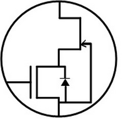
Figure 1: USCi cascode combines a Si MOSFET with SiC JFET in a single TO-247 package
The driving force for power switch paralleling generally requires greater current and power capacity by employing a single power switch. Also, applying parallelled TO-247 cascodes yields flexibility in system implementation that is difficult to attain with prepackaged modules. This flexibility enables optimization of tradeoffs between switching and conduction losses, thermal design, cost, and system performance based on the requirements of a specific circuit topology and application. To realize these benefits, SiC cascodes can be paralleled with the same basic approach used to parallel silicon MOSFETs.
A primary difference between operating a single power switch and multiple parallel switches is the need to account for any current and power dissipation imbalance when verifying that the device is used within its safe operating area. For SiC cascodes, the level of current and power dissipation imbalance is minimal and the devices may be used without significant derating provided some basic precautions are followed. In particular, adequate consideration should be given to gate drive design and power circuit layout to minimize sources of imbalance.
The following sections discuss the parallel gate drive scheme; current imbalance during conduction, turn-ON, and turn-OFF; and practical tips for implementing paralleled SiC cascodes. Measurement results of current sharing of United Silicon Carbide’s UJC1206K cascode are included. These measurements were made with a shunt resistor at the source node and include the gate current in addition to the drain current. For clarity, the case of two parallel cascodes is illustrated. The concepts are easily extended to paralleling of larger numbers of devices once they are understood for the two-switch case.
Gate Drive for Parallel Cascodes
A notional schematic of a suitable gate driver circuit for parallel cascodes is shown in Figure 2. A separate RGon and RGoff are used so that the turn-on and turn-off switching transitions can be independently controlled. For parallel operation, the most important gate drive consideration is that separate gate resistors be used for each of the paralleled devices. When paralleling only a few cascodes the optimum design uses a single gate driver for all of the paralleled devices. On the other hand, when driving a large number of parallel cascodes separate buffers for each switch will enable compact gate control loops, which will reduce gate loop inductance. The layout of the cascodes themselves should allow for low and well-matched stray parasitic inductance, particularly in the source connection. With low source inductance, a good source Kelvin connection can be used at the cascode device leads.
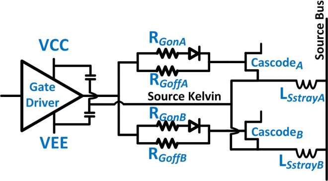
Figure 2: Notional Schematic of Parallel Gate Drive
Power Balance During Conduction
In steady state conduction, paralleled cascodes share a common VDS and each cascode conducts current in proportion to its RDSon. Like silicon MOSFETs, SiC cascodes have a positive RDSon versus temperature characteristic (Figure 3). The positive temperature characteristic performs an important role as it provides negative feedback from a cascode’s power dissipation to the amount of load current it conducts in parallel operation.
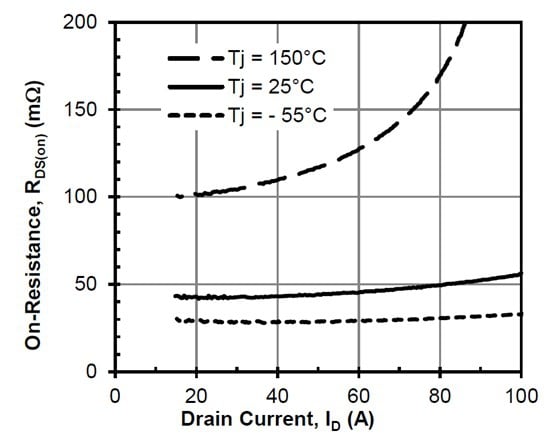
Figure 3: SiC Cascode RDSon versus Temperature Characteristic
To understand this feedback effect, consider two cascodes, denoted Cascode A and Cascode B, biased at a fixed VDS. At startup, if Cascode A has lower RDSon than Cascode B, Cascode A will conduct a higher percentage of the load current than Cascode B. This will increase Cascode A’s temperature relative to Cascode B. The higher temperature increases for Cascode A leads to higher RDSon increase for Cascode A which lowers the percentage of load current through it. The end result is more balanced current sharing in steady state between Cascodes A and B. Notably, this behavior prevents thermal runaway which can occur with other switch technologies due to their positive on-resistance temperature characteristics.
To determine the startup and steady state conduction current sharing in detail the datasheet RDSon temperature characteristic, the device thermal impedance, and the parallel switch voltage and current conditions can be used to model the interdependence of RDSon, temperature, and current sharing. This same analysis can be used to study sensitivity of the device conduction to any expected variations in thermal resistance. For this electrical and thermal analysis, the device datasheet thermal impedance information can be used as a starting point but final modeling should include the actual system thermal impedance as determined by simulation and measurement of the thermal characteristics of the actual system.
Power Balance During Switching
Turn-ON: During cascode turn-ON (illustrated in Figure 4), at t1VGS begins to rise at a rate determined by the time constant formed by the gate resistor and the cascode input capacitance (RGonCiss) and the gate driver power supply voltage. When the VGS value exceeds the cascode threshold voltage at t2, the device turns on and after a small delay the drain current increases at a rate influenced by the gate resistor and source inductance. The drain current di/dt causes a voltage rise across internal package inductance, which is capacitively coupled from the source to the gate and reflected in the VGS waveform as measured at the TO-247 leads. At t3, the drain current is fully commutated and VDS falls. The turn-ON switching loss is the integrated product of VDS and ID and over the switching interval
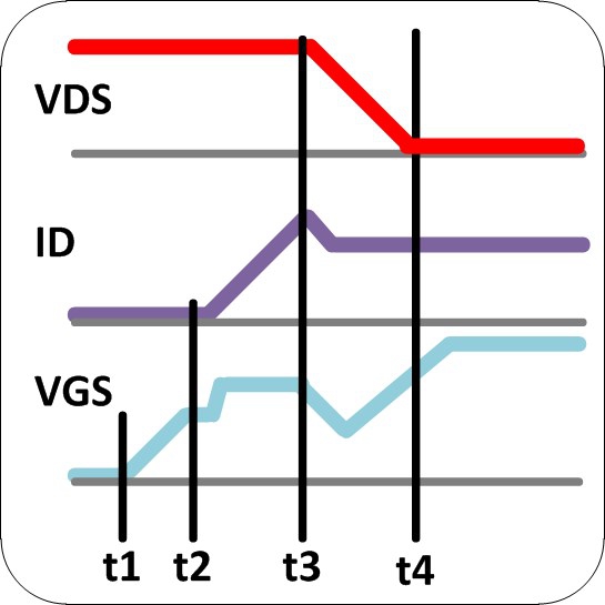
Figure 4: Cascode turn-ON behavior for a single device
For paralleled devices with matched stray inductance, VDS falls in parallel for all the cascodes and does not affect the power balance between devices; any turn-ON power imbalance results from differences in current sharing during the switching time. Also, when paralleled cascodes are turned ON, matching of the di/dt rate can be assured by matching the parasitic source inductance and gate resistance. The source inductance matching can be controlled through identical layout from each cascode source lead to the associated bus. The gate resistors can be easily matched with available low cost, high tolerance resistors.
With common VDS falling and matched di/dt, the potential for mismatch in the turn-ON loss still exists if there is a skew in turn-ON delay between the paralleled switches. Using a single gate driver helps minimize any turn-ON delay skew by eliminating potential gate driver propagation delay variations. As discussed above, turn-ON begins when VGS exceeds the cascode threshold voltage and the rate of VGS rise prior to cascode turn-ON is controlled by the time constant RGonCiss and the gate driver power supply voltage. Since the cascode Ciss is well matched between devices, the gate resistors can have tight tolerance, and the gate driver power supply voltage is common across paralleled devices the VGS rises uniformly for paralleled devices prior to turn-ON. Therefore the primary contributor to turn-ON delay skew is the variation in cascode threshold voltage.
Figure 5 shows the turn-ON current sharing for two well-matched cascodes and two cascodes, which were selected as they had the highest threshold variation (150 mV) in the samples tested. The third plot in Figure 5 shows the turn-ON when there is large temperature imbalance of 25 °C and 65 °C between the devices under test. As shown, even with variation in threshold voltages and temperature, the turn-on current sharing, and therefore switching loss, is very well matched between devices. At the beginning of the conduction period a significant difference exists in the current load as the results are from a double pulse test, which does not allow sufficient time for the RDSon temperature dependence balancing to take effect.
The small impact of threshold voltage variation results from the low variation in cascode threshold voltage (+/- 200 mV typical) and the gate loop behavior, which dampens the effect of variations in device characteristics.
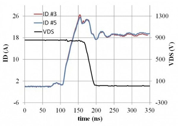
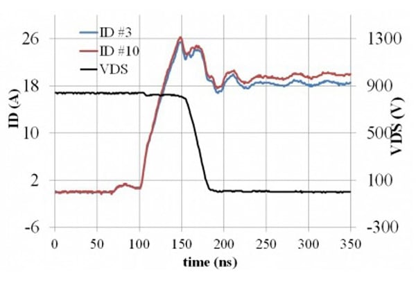
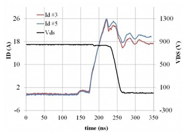
Figure 5. Turn-ON current sharing at 850 V, 18A: top) matched cascodes, middle) mismatched threshold voltages, and bottom) 40 °C temperature offset between devices.
For example, consider the case where Cascode A and Cascode B have threshold voltages of 4.3 and 4.7 V respectively. During parallel turn-ON, the VGS of Cascode A will reach threshold first and it will begin to turn-ON. As soon as it turns ON the di/dt across the inductance internal to the Cascode A package causes an increase in the VGS as measured at the pins of the TO-247 terminals. This causes a drop in the gate current due to the lower voltage across the gate resistor. Meanwhile, Cascode B still has a relatively low gate voltage and its VGS continues to slew with higher current. Based on the slew rate of the gate driver near threshold, the delay between the turn-ON of Cascode A and Cascode B for the large threshold voltage variation of 400 mV is only 0.6 ns. With a di/dt of 1 A/ns this leads to less than 600 mA of current mismatch during turn-ON due to threshold mismatch. For a 20 A load current this results in a 6% mismatch in current sharing. For lower load currents, the mismatch percentage is higher but is not usually of concern, as it does not affect the safe operating area analysis due to operation well within the specified device limits. Turn-OFF: During turn-OFF (illustrated in Figure 6) at t1 the gate driver switches low and VGS begins to fall towards the cascode threshold voltage. At t2, VGS plateaus as the MOSFET inside the cascode reaches its miller plateau. At t3, the delay time ends and the VDS transition begin. The overall effect of the turn-OFF delay interval on the turn-OFF loss imbalance is analogous to the turn-ON case: close matching of Ciss, gate resistor, and gate driver supply voltage results in the threshold voltage mismatch dominating the turn-OFF delay mismatch and the end result is only a marginal effect on the switching loss imbalance. However, in the case of turn-OFF there are some additional considerations.
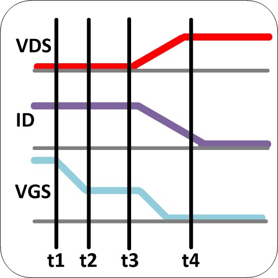
Figure 6: Turn-OFF switching behavior
First, at the start of turn-OFF there may already be a current imbalance due to differences in RDSon between paralleled devices. This difference in the conduction current will lead to a different current level in the parallel devices at the start of the turn-OFF process. As shown in Figure 6, VDS rises during the turn-OFF current transition so this current imbalance creates a switching loss imbalance between the paralleled devices.
Secondly, at high current levels and high dv/dt the cascode’s internal response is underdamped which can lead to turn-OFF current ringing. The ringing does not necessarily lead to high cascode loss but it is coupled to the VGS signal at the TO-247 leads through the common source inductance and it may be unacceptable at the system level. Any current ringing may also lead to imbalanced operation between paralleled cascodes as the di/dt it generates interacts with stray inductances, which may not be perfectly matched. If the combination of high current and stray inductance lead to this problem it can be controlled through increase in the value of RGoff or the addition of a small capacitor between the gate and drain terminals of the cascode. In general, the additional CGD is the preferred method, as it will provide good dv/dt control without adding to the total turn-OFF delay or impacting turn-OFF delay skew as would happen with large values of RGoff.
The measured turn-OFF behavior is shown in Figure 7 for pairs of devices with matched (top) and mismatched (middle) thresholds. A plot (bottom) is also included where one device is heated to 65 °C to generate a current imbalance to illustrate the potential current ringing behavior.
When considering the impact of turn-OFF loss imbalance, it is important to consider that the turn-OFF switching loss magnitude is much less than the turn-on and conduction losses in hard-switched applications. This means that even a high turn-OFF loss imbalance may not significantly affect the overall power imbalance. Also, any imbalance in current sharing during the turn-OFF interval is short lived and unlikely to exceed the devices safe operating conditions.
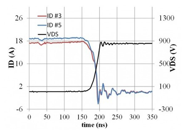
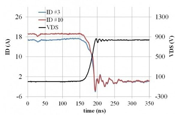
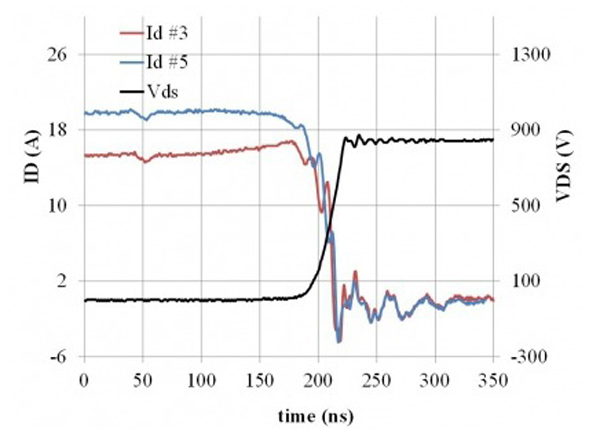
Figure 7: Turn-OFF current sharing at 850 V, 18A: top) matched devices, middle) mismatched devices, bottom) 40 °C temperature offset between devices
Implementation Tips
- The cascode’s positive RDSon temperature dependence helps ensure good current and power sharing during conduction. A common heat spreader or heatsink for paralleled switches will help leverage this effect. As with silicon MOSFETs, there can be a residual conduction current imbalance, which should be accounted for when verifying device operation is within the specified safe operating area.
- Turn-ON current and power imbalance is minimal and depends primarily on the MOSFET threshold voltage variation. The current imbalance will be limited to the di/dt multiplied by the turn-ON delay mismatch value. With matched switch leg layouts, a typical threshold voltage mismatch of +/- 200 mV, RGon = 5 Ω, and a 12 V gate driver supply will lead to a turn-ON delay mismatch of less than 0.6 ns. With a turn-ON di/dt of 1 A/ns the resulting current mismatch is less than 600 mA.
- Cascode turn-OFF loss is more susceptible to mismatches in percentage terms than turn-ON losses due to the added effect of differences in conduction current and coincident voltage rise and current fall times. In extreme cases the turn-OFF may exhibit current ringing, which is also seen in the VGS signal as measured at the TO-247 leads. To control the current ringing, large gate turn-OFF resistors values may be used if increase in turn-OFF delay is acceptable. Alternatively, a small value capacitor can be added to the cascode gate to drain connection to slow the turn-OFF without increasing the turn-OFF delay time. While the turn-OFF loss sharing may have a significant percentage mismatch between devices the turn-OFF loss magnitude is low compared to turn-ON and conduction losses so the overall impact of turn-OFF balance on device power dissipation imbalance may not be significant.
- For a small number of parallel devices a single gate driver with separate gate resistors for each switch will provide the best current and power balance. For large numbers of devices in parallel, gate drive buffers for each switch may lower the gate loop area and inductance. If separate gate drive buffers are used a simple single stage common emitter buffer should be considered over a complete gate driver IC due to the potential contribution of gate drive propagation delay skew.
- In the power loop layout the TO-247 packages can be closely spaced with DC decoupling capacitors to lower the overall power loop inductance. For best matching, variations in the layout that can lead to difference in stray inductance should be avoided, especially at the source lead.
Conclusion
Theory and lab testing demonstrates the inherent capability of SiC cascodes to be safely paralleled. Due to the characteristic behavior and low production parametric variations of USCi’s cascodes part screening is not required for paralleled operation. The worst-case current and loss imbalance can be determined for a given system and operation within the cascode safe operating area can be verified in order to avoid over margining of designs.
About the Authors
Matt O'Grady works as the Director of Applications at USCi, a company that develops innovative silicon carbide FET and diode power semiconductors that deliver the industry’s best SiC efficiency and performance for electric vehicle (EV) chargers, DC-DC converters and traction drives, as well as telecom/server power supplies variable speed motor drives and solar PV inverters.
Ke Zhu works as an Application Engineer at United Silicon Carbide, Inc. where his duties cover developing demonstration circuits to facilitate the use of USCi devices in various applications and provide customer application support as well as writing application notes and technical papers to explain the benefits. He holds a Bachelor's Degree in Electrical Engineering earned at Chongqing University and a Master's Degree in ECE earned at the Ohio State University.
John Bendel works as the Senior Director for Business Marketing at United Silicon Carbide, Inc. since May 2014 where he is skilled in the field of semiconductors and power management. He earned his Bachelor's Degree in Electrical Engineering at the University of California, Davis.
Xueqing Li received the B.S. degree in electrical engineering from Tsinghua University, Beijing, China, in 1990, the M.S. degree in physical electronics and optoelectronics from the Institute of Electronics, Chinese Academy of Sciences, Beijing, in 1993, and the PhD degree in electrical and computer engineering from Rutgers University, Piscataway, NJ, in 2005. Since 2003, he has been a Senior Research Engineer with United Silicon Carbide, Inc., New Brunswick, NJ, where he is responsible for the design and simulation of power devices in 4H-SiC, creation of PSpice model of power semiconductor devices, and simulation of switching-mode power converter systems.
References
- Bendel, John and Li Xueqing, “Using “Normally on” JFETs in Power Systems,” Magazine of Bodo’s Power Systems, March 2015, pp.40-43.
- Bhalla, Anup; Bendel, John and Li Xueqing, “Switching Behavior of USCi’s SiC Cascodes” Magazine of Bodo’s Power Systems, June 2015, pp.22-26.
- Aggeler, D.; Biela, J.; Kolar, J.W., “Controllable dυ/dt behaviour of the SiC MOSFET/JFET cascode an alternative hard commutated switch for telecom applications,” APEC 2010 IEEE pp.1584,1590, 21-25 Feb. 2010
- Forsyth, J., "Paralleling Of Power MOSFETs For Higher Power Output", http://www.irf.com/technical-info/appnotes/para.pdf
- Wu, Y.F., "Paralleling high-speed GaN power HEMTs for quadrupled power output," APEC 2013 IEEE pp.211-214, 17-21 March 2010