Facebook
 Google
 GitHub
 Linkedin
The Next Generation of High Power IGBT Modules
This article highlights Mitsubishi Electric Europe B.V LV100 High Power IGBT Modules for Wind Converter, Photovoltaic Inverter and Motor Drives.
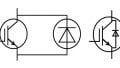
LV100 for Wind Converter, Photovoltaic Inverter and Motor Drives
High power applications in the fields such as renewable energy and industrial drives require reliable and scalable power modules with high power density and low stray inductances. In order to fulfill these requirements, the concept of the well-known and successful HVIGBT LV100 package has been transferred and adapted to the needs of renewable and industrial applications.
LV100 Concept
Applications like wind energy converters, central photovoltaic inverters and industrial drives require power modules with the highest power density, high reliability, and scalable power ranges with a standardized outline in the voltage classes of 1200V and 1700V. To fulfill such requirements, the LV100 power module is based on the same outline and internal layout concept as the well-known HVIGBT LV100 module.
Efficient Chips and the Thermal Cycle Failure Free SLC-package-technology
This concept is convincing because it is based on a standardized package outline while also capable of delivering the highest power density, scalability by easy paralleling, low stray inductance, capability to operate with fast switching devices like SiC MOSFETs and having excellent current sharing balance. In combination with the latest 7th generation IGBT and Diode efficient chips and the thermal cycle failure free SLC-package-technology, the LV100 module provide the best overall performance. In the 1700V, a current rating of 1200A has been realized which represents an outstanding current density considering the compact package footprint of only 144x100mm².
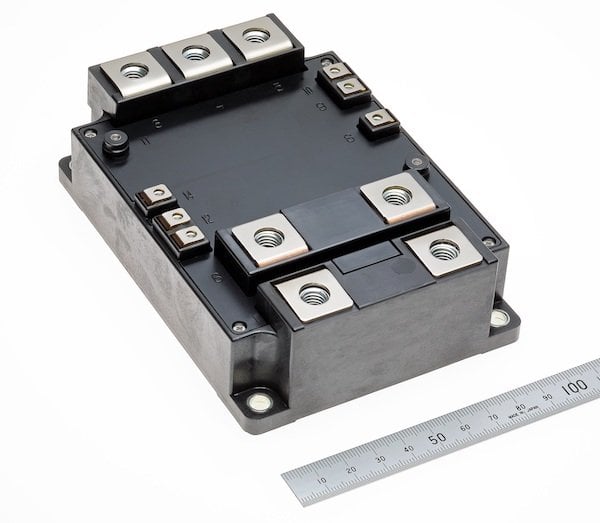
Figure 1: New LV100 Power Module for industrial application
LV100 Internal Layout
In high power IGBT modules, multiple chips are connected in a parallel configuration because IGBT chips sizes are limited and usually the rating maximum current is in a range of ~200A for IGBT chips with blocking voltages of 1200V or 1700V.
Achieving Homogeneous Loss and Heat Distribution
Therefore, for the realization of an IGBT module with a current rating of 1200A or more, paralleling of at least six or more IGBT chips is required. While designing the layout, the current balancing between the chips connected in parallel has to be considered. Equally shared chip currents are required for achieving homogeneous loss and heat distribution. A non-homogeneous current distribution causes a certain chip to carry the highest current and this chip will experience the highest temperature which ultimately limits the performance and life-time of the total system.
Parasitic Impedances of the Connection
The parasitic impedances of the connection to the individual chips significantly influence the current sharing between the chips operated in parallel. In case the parasitic inductances are not equally designed for all chips, a dynamic current imbalance during IGBT switching will occur. The module terminal arrangements and the chip positions are the major influencing factors for the parasitic impedances. To realize an equal impedance, the distances from the power terminals to all the chips have to be ideally the same.
This can be achieved by optimizing the terminal and chip arrangement so that it is perpendicular to the current flow as shown in figure 3 [6]. In the ideal module concept, the commutation (indicated by the blue and red arrows) is only in Y-direction whereas the terminals and chips are orientated perpendicular in x-direction.
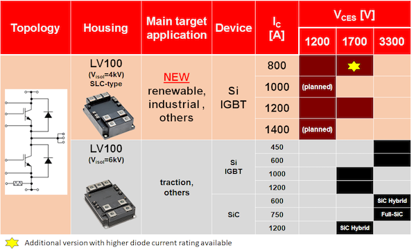
Figure 2: LV100 product line-up plan
By this approach, equal parasitic impedances are achievable. This ideal concept was considered in the development of the LV100 layout and a homogenous current sharing, as shown in the simulation result in figure 4 was realized.
Conventional Modules
The conventional modules available today in the field of high power industrial drives or converters for renewable energy usually have a terminal arrangement which is parallel to the chip arrangement and current flow. As a result of this conventional design, equal parasitic impedances was not be realizable and the resulting imbalance in the current sharing was an accepted feature of the conventional modules. For events such as load short circuits, due to the absence of the inductive coupling in the laminated busbars, the impact of the unequal stray inductances between different chips becomes significant for such conventional modules.
SiC Devices
In case of fast switching semiconductor devices with high di/dt, the differences in parasitic stray inductances between the chips will influence the current sharing enormously. Therefore, if an inverter designer considers changing to SiC devices in future, the LV100 package is the right choice since the layout concept is ready for SiC [8]. As result, a potential future change from Si-IGBT to SiC-MOSFET [9] devices is feasible with less changes and redesign efforts.
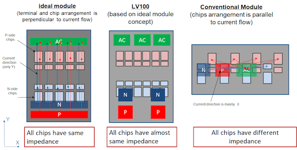
Figure 3: Comparison of power module layout concepts
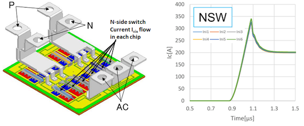
Figure 4: Simulation result of current sharing at turn-ON event in LV100 package concept.
Thermal cycle failure-free package
IGBT modules in high power industrial drive applications experience thermal cycling [1] in case of fluctuating (or non-continuous) loads. Wind power converters are usually liquid-cooled with the cooler having a thermal time constant of a couple of seconds. As a result, the IGBT case temperature will respond rapidly to a temperature swing by changing of load conditions. That means on days with fluctuating wind conditions the IGBT module baseplate will experience many thermal cycles. Also photovoltaic inverters experience at minimum one huge thermal cycle per day. Considering an inverter life-time of 25 years, the IGBT module have to be capable to resist several thousand thermal cycles.
The thermal cycle capability of conventional industrial IGBT modules with conventional package structure (with several pieces of ceramicling substrates solder to copper baseplates), is limited. Hence thermal cycles have to be considered as lifetime limiting parameter during the converter design. To eliminate thermal cycling as lifetime limiting parameter, the SLC-Technology [2] [3] has been selected for the LV100 development for industrial application. As shown in figure 5, the conventional power module package structure is replaced by an IMB (Insulated Metal Baseplate) in combination with a direct potting resin.
The thermal expansion coefficient of the insulator and the potting resin are matched with each other [4] (considering the thermal expansion of copper base- and pattern-layer. Due to this matching thermal expansion and the elimination of system solder layer, a thermal cycling failure free package structure has been realized [5].
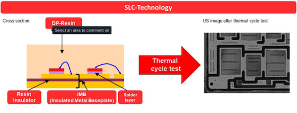
Figure 5: SLC-Technology and thermal cycle test result
7th gen 1700V IGBT chip-set
The 7th gen IGBT and diode chips possess an optimized structure and are thinner than its predecessors. Additionally, the devices have been designed by selecting an appropriate trade-off between the DC performance and the switching performance [5].
The inverter losses under typical application conditions for high power converters has been performed by Mitsubishi Electric Melcosim [7] simulation software. In figure 6 the result and comparison of 1200A/1700V LV100 vs a conventional 1400A/1700V module from company A. It is noticeable that for a switching frequency of 500Hz the total losses are comparable. However, due to the appropriately selected trade-off in combination with the optimized chip structure, the diodes and the IGBTs indicate switching losses are significantly reduced.
The result is that for switching frequencies higher than 500Hz, the LV100 has significantly higher efficiency. For example, at a switching frequency of 5kHz the loss reduction is 39%. This loss reduction contributes to reducing the cost of the total inverter by reducing efforts for cooling and enabling to achieve higher power density of the system.
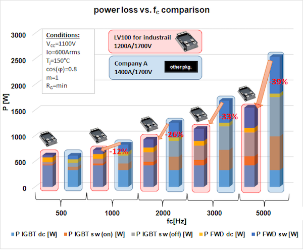
Figure 6: Power loss comparison of 7th gen. IGBT chip in LV100 1200A/1700V module vs. Company A 1400A/1700V conventional module.
Conclusion
A new high power IGBT module (LV100 for industrial) is under development, which has been optimized for the requirements of high power applications in the field of renewable energy converters, and industrial drives. The outline of the module housing is same as HVIGBT LV100 and in line with the new market defacto standard. The SLC-package-technology is thermal cycling failure free and improves the reliability of the system.
The 7th gen IGBT chip technology provides a significant reduction of switching losses and is beneficial considering a switching frequency from 500Hz onwards. The internal layout has a minimized stray inductance and ensures a homogenous current sharing between the chips. Therefore, it is feasible to use this layout with fast switching semiconductor.
About the Authors
Thomas Radke is a Senior Application Engineer at Mitsubishi Electric Europe B.V, a company branch of Mitsubishi Corporation that focuses on electronics and electrical equipment manufacturing located in Ratingen, Germany. He earned his Bachelor's degree in Electrical Engineering and Electronics at Fachhochschule Düsseldorf (University of Applied Sciences - Dusseldorf). He also acquired his diploma in Associate Engineer in Automation Technology at Siemens Technology Academy - Düsseldorf.
Narender Lakshmanan works as an Application Engineer at Mitsubishi Electric Europe B.V, Ratingen, Germany. He is responsible for power semiconductor-based power converter solutions and has past roles which include project management of EPC projects. He earned his Bachelor's Degree in Electrical Engineer at Anna University, Chennai, Tamil Nadu, India. He then acquired his Master's degree in Electrical Power Engineering at RWTH Aachen University, Aachen, Germany.
References
- “Power Module Reliabilty” Mitsubishi Electric Application note Power Module Reliability PDF
- T. Takahashi, et al: “A 1700V-IGBT module and IPM with newinsulated metal baseplate (IMB) featuring enhanced isolationproperties and thermal conductivity”, PCIM Europe 2016
- S. Asada, et al: “Resin Encapsulation Combined with InsulatedMetal Baseplate for Improving Power Module Reliability”, PCIMEurope 2016,
- J. Yamada, et al: ”Pumping out failure free package structure”,PCIM Europe 2016,
- Thomas Radke et. al., “More Power and Higher Reliability by 7th Gen. IGBT Module with New SLC-Technology”, Bodo’s PowerSystems June 2015[5]M. Miyazawa, et al: “Mitsubishi 7th generation 1700 V IGBT Modules: Loss Reduction and Excellent System Performance”, Bodo’sPower Systems March 2018
- Georg Borghoff, “Implementation of low inductive strip line con-cept for symmetric switching in a new high power module”, PCIMEurope 2013, p. 185
- Melcosim simulation software for Mitsubishi Electric power modules Melcosim Simulator
- N. Soltau, et al: “3.3 kV Full SiC MOSFETs - Towards High-Performance Traction Inverters,” Bodo’s Power Systems, pp. 22-24,Jan. 2018[9]N. Soltau, et al: “Switching Performance of 750A/3300V Dual SiC-Modules”, Bodo’s Power Systems, pp. 26-28, Feb. 2019
This article originally appeared in the Bodo’s Power Systems magazine.