Facebook
 Google
 GitHub
 Linkedin
LinPak – the new Standard Phase-Leg Module with Exceptional Low Inductance
This article introduces ABB Semiconductor's LinPak, a new IGBT module generation that is the enabler for lowest overall stray inductance.
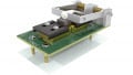
One year ago ABB presented the LinPak, a new IGBT module generation that is the enabler for lowest overall stray inductance. In the meantime the LinPak module with a footprint of 100 x 140 mm2 has established itself as a new standard. The ABB lineup of LinPak modules starts with a module rating of 1700V and 2x1000A. This spring ABB will complement the LinPak family with a 3300V and 2x450A rated module.
The LinPak IGBT module features an exceptionally low stray inductance enabling the full utilization of advanced low switching loss IGBT chipsets and even future full silicon carbide switch solutions. In addition the LinPak is ideally suited for parallel connection with negligible derating, thus allows for a large range of inverter powers with just one module type. Together with the open standard concept this module fulfills a long wish of the industry in nearly all high-power segments such as traction & CAV (commercial, construction and agricultural vehicles), wind & solar and industrial drives to name a few.
Present IGBT module solutions are at its limit when it comes to advanced and faster IGBT/diode chipsets since the overall stray inductance per switched ampere is too large and high over-voltage will occur. In addition, the available electrical contact area of today’s modules is limited and dates back to times when the packages were rated with 50% less current than now. Due to today’s modules’ lack of scalability, a large variation of outlines exists to match various inverter ratings. The presented LinPak module concept solves all these issues and is published as an open standard. Several module manufacturers have adopted the outline and customers benefit from a standard solution. The LinPak offers as well exceptional low package stray inductance of 10nH and an easy customer interface enabling the construction of a very low-inductive DC-connection with sufficient contact area for the high current densities. This is the ideal fit for the full utilization of the advanced fast IGBT/diode chipsets such as the latest 1700V SPT++ technology. It also makes the package fit for future hybrid and full SiC solutions that come with much higher switching speeds.

Figure 1: ABB’s low-inductive LinPak IGBT module for reliable high-power converters
Beside the very advanced and novel package concept, the LinPak features ultra-sonic welded terminals and an advanced high reliability solder joint between the unrivaled AIN substrate and AlSiC baseplate material combination. In addition, the well-established high temperature cycling capable bonding technique and the gate-print to substrate aluminum bond interconnect from the improved HiPak are incorporated in the new LinPak design.
Application benefits
Module scalability and record current density
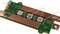
The LinPak module type offers the benefit that just one module type is needed per voltage rating. Thanks to a homogenous current path concept, the module enables parallel connection of more than four modules without any significant derating (Figure 2).

Figure 2: LinPak scalability
The current density of LinPak modules offers a solid improvement of more than 10% compared to older module types on the market as shown in Table 1.
| Module Type | Current Rating | Foot-print | Current / Area |
| LinPak | 2 x 1000A | 100 x 140mm2 | 14.3 Acm-2 |
| HiPak | 3600A | 140 x 190mm2 | 13.5 Acm-2 |
| PrimePACK | 2 x 1400A | 89 x 250mm2 | 12.6 Acm-2 |
Table 1: Current density of LinPak compared to other module types
Mechanical concept and connections
The gate-unit connection for the LinPak is realized with a simple adapter-board (PCB) directly mounted onto the module between AC and DC terminals. The connection to the auxiliary terminals for gate, emitter, collector and thermistor are realized with M3 screws. In addition, four molded M3 nuts are positioned in the corners to mechanically fix the adapter board for harsh environmental applications like traction or CAV. The adapter-board connects the modules’ gates and auxilliary emitters in parallel. Thus, many modules can be connected in parallel with just one gate-unit.
The NTC thermistor is located in the center of the module and thus allows a fast monitoring of the module base-plate temperature. Optionally auxiliary emitters that tap the potential of the power emitter connection on the Minus-DC and Phase-Terminal can be equipped. Those 2nd auxilliary emitters can be used to sense the inductive internal voltage drop during fault conditions. This allows the gate-drive unit to react faster to short-circuit events and trigger protective functions.
The power connections are designed to enable an absolute symmetrical DC-connection, which is crucial for excellent current sharing. The creepage and clearance distances are designed according to IEC 60664-1 and EN 50124-1 for functional insulation up to a device rating of 3300V.
Power connections
The LinPak offers the highest contact area per rated current. Table 2 compares the current per M8 screw for various packages. To compare the various package types, the phase current is calculated by dividing the device’s nominal current by √2.
| Module Type | Nominal Type | Phase current | Amp / M8 screw (phase terminals) |
Amp / M8 screw (DC terminals) |
| LinPak | 1000A | 707A | 354A | 250A |
| PrimePACK | 1400A | 989A | 495A | 350A |
| HiPak | 3600A | 2546A | 600A | 600A |
Table 2: Current per M8 screw connection
Because of the large contact area offered by the LinPak, heating of the contact interface and the terminal itself is much reduced compared to HiPak or PrimePACK modules. For future chip generations with even further increased current densities, the LinPak offers space between the existing phase-connections to accommodate a third AC-connection which reduces the contact resistance from bus-bar to module even further.
Record low stray inductance
Present module designs have rather high stray inductance values causing high over-voltages. This makes the use of advanced fast chipsets – such as the ABB 1700V SPT++ chipset – difficult and the use very fast future SiC solutions close to impossible.
The LinPak is designed to offer the lowest internal stray inductance current thus enabling low inductive bus bars. Figure 3 compares the LinPak with a HiPak including a bus bar and an assumed DCcapacitor inductance of 1.5nH. Still, when including the bus bar and capacitor, the over-voltage is below critical levels compared to the HiPak solution – even with fast chipsets. This makes the LinPak the ideal candidate for parallel connection up to high current applications without compromising the switching losses.

Figure 3: Stray inductance including bus bar
Electrical results
The 1700V, 2x1000A rated LinPak modules have been tested in a real application environment with laminated bus bars. The achieved stray inductance is below 25nH. As a result, the measured waveforms figure 5 to 7 show exceptional smooth switching characteristics and very low voltage overshoots, this despite the very fast and low-switching losses SPT++ chipset.
This renders obsolete the need for sophisticated gate-units with active clamp circuits that are always critical for gate-driver reliability. As a prove figure 6 shows the IGBT safe operating area (SOA) with double nominal current turn-off to a high DC-link voltage of 1300V without active clamp. Thanks to the low inductive design of the LinPak the over-voltage even under this extreme conditions stays below 1700V!


Figure 4a: Nominal IGBT turn-on (top) Nominal IGBT turn-off (bottom)

Figure 5: Nominal Diode recovery

Figure 6: IGBT SOA at double nominal current

Figure 7: IGBT short-circuit ruggedness
Conclusions & Outlook
The LinPak is a new open standard module that satisfies the requirements posed by both new advanced fast and high current density chipsets as well as customer wishes for a flexible and scalable IGBT module that is, in addition, ready for future technologies such as SiC devices. The benefits of the novel low stray inductance LinPak IGBT module are clearly demonstrated and measurements confirmed the expectations from the new module. Today, the benefits of the new package enable customers to profit from the latest chip technologies with low-inductance for achieving the highest current density. Furthermore, particle-free ultrasonic welding of the main terminals, advanced wire bonding including the well-established and unrivalled AIN / AlSiC substrate/baseplate material combination for high-temperature cycling capability are incorporated. At PCIM 2016 in Nuremberg ABB will present the 3300V LinPak version including results from the electrical verification.
About ABB
ABB is a pioneering technology leader with a comprehensive offering for digital industries. With a history of innovation spanning more than 130 years, ABB is today a leader in digital industries with four customer-focused, globally leading businesses: Electrification, Industrial Automation, Motion, and Robotics & Discrete Automation, supported by its common ABB Ability™ digital platform. ABB's market-leading Power Grids business will be divested to Hitachi in 2020. ABB operates in more than 100 countries with about 147,000 employees.
References
- Raffael Schnell, Samuel Hartmann, Dominik Trüssel, Fabian Fischer, Andreas Baschnagel, Munaf Rahimo, “LinPak, a new low inductive phase-leg IGBT module with easy paralleling for high power density converter designs” Proc.PCIM’15 Nuremberg, 2015
- Raffael Schnell, Munaf Rahimo “The Quest for Higher Switching Frequency and its Implications on Semiconductor Switches” Proc. PCIM’11 Nuremberg, 2011
- Corvasce C., Kopta A., Rahimo M.T., Schnell R, Geissmann S., Vobecky J.; “New 1700V SPT+ IGBT and Diode Chip Set with 175°C Operating Junction Temperature” EPE’2011, BIRMINGHAM, UK, Aug. 2011
- R. Schnell, U. Schlapbach, K. Haas, G. Debled, “Parallel Operation of LoPak Modules” Proc. PCIM’03 Nuremberg, 2003.
- G. Borghof “Implementation of low inductive strip line concept for symmetric switching in a new high power module”, PCIM’13 Nuremberg, 2013
This article originally appeared in the Bodo’s Power Systems magazine.