Facebook
 Google
 GitHub
 Linkedin
High Efficiency IGBT M7 Chip Technology utilized in the Mid Power Package VINco E3
This article highlights Vincotech M7 chip and the SLC package technology utilized by VINco E3 product line for an efficient and reliable mid-power package.
Power semiconductors are the core components of any energy conversion system and are essential for the efficient utilization of energy. Achieving minimum power loss is one of the most critical goals in the development and use of power semiconductors, and it is fundamental for meeting the market demands for saving energy. Low radiation noise, wide safe operation, and high reliability are additional key development goals.
Current silicon-based semiconductors are approaching their physical limits in terms of physical properties. However, there is still room for improvement and semiconductor engineers are working on this continuously. As a result, Mitsubishi Electric has recently introduced the M7 chip technology, its latest generation. Using new technologies, such as ultra-thin wafer processing and new backside doping techniques, they have achieved their goal of improving usability for industrial applications.
Power module packaging technology plays a vital role in ensuring optimal utilization of this new chip technology. VINco E3, a new mid-power package based on the so-called SoLid Cover (SLC) technology, has been developed with high thermal cycling capability and full compatibility to the standard industry packages. Higher thermal cycling capability helps increase reliability and lifetime, and compatibility with standard packages ensures ease of use and optimize manufacturing costs. The new M7 chip technology and optimized VINco E3 packaging offer a powerful combination to meet the demands of the market. This article will describe the core features of the new M7 chips and the new VINco E3 package and the benefits of this combination based on an application benchmark.
Features of the new M7 chip technology
IGBTs
For the IGBT M7, Mitsubishi Electric is using the same carrier stored trench-gate bipolar transistor (CSTBT) structure as used in gen 6. The IGBT M7 has been improved through ultra-thin wafer processing, resulting in significantly reduced the VCEsat and associated losses. Figure 1 is a comparison of VCEsat between the IGBT M7 and the best competitor, and clearly shows more than 20% (@600 A Ic) lower conduction power losses for the IGBT M7.
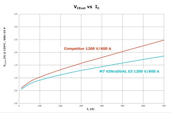
Figure 1: IGBT M7 vs competitor: VCE as a function of IC at 105°C TJ
Usually an IGBT optimized for very low conduction losses would have higher switching losses and vice versa, Figure 2 clearly shows that the IGBT M7 offers both lower switching losses and lower conduction losses. The benchmark was done with the new VINcoDUAL E3 package which is described also in this article. This improvement in both VCEsat and Eoff/Eon leads to a reduction of the total power losses. By thinning the wafer, there is an increased risk of reducing the safe operating area (SOA) capability of the device. However, this risk has been eliminated by the optimization of the MOS structure (gate capacitance). In addition to the improved SOA capability, the controllability (dv/dt) of the device with the gate resistance has been improved compared to gen 6.
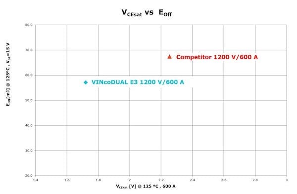
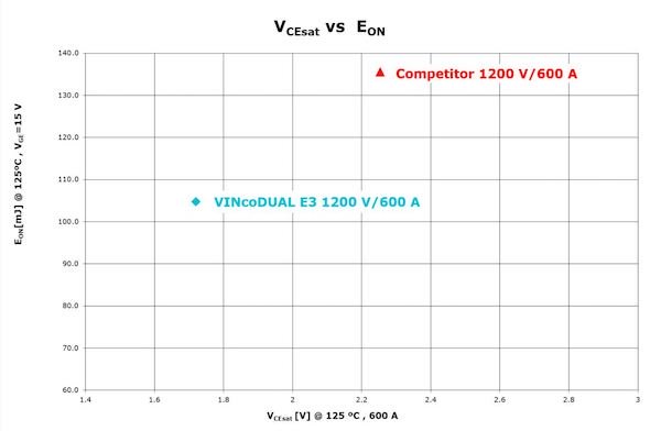
Figure 2: IGBT M7 vs competitor: Improvement in VCEsat and Eoff/Eonleads to a reduction of the total power losses
Diodes
The M7 diodes, compared to the conventional diffusion wafer diodes, have been developed with the new Relaxed Field of Cathode (RFC) technology adopting a new backside structure and thinner wafer technology. However, reducing the chip thickness increases the risk of chip destruction due to stronger snap-off reverse recovery behavior. This risk has been eliminated with the RFC technology. The turn-ON switching waveform of the M7 diode in Figure 3 shows a lower current overshoot and less oscillation compared to the competitor diode. This allows EMC to be optimized and total system costs can be reduced. An additional benefit of the thinner wafer is reduced the forward voltage (Vf) drop. From gen 6 to gen 7, the Vf has been reduced by approximately 20%.
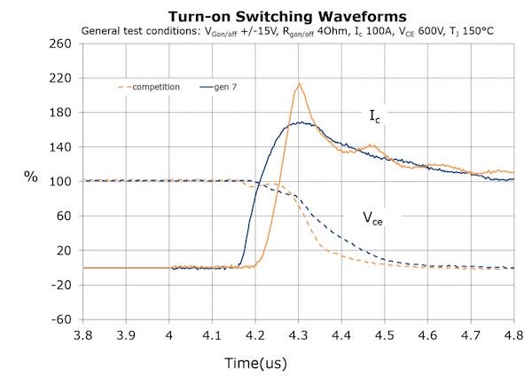
Figure 3: M7 diode vs competitor: Turn-ON switching waveform
The RFC structure of the M7 diode significantly improves the Erec without the usual increase in Vf, as seen in Figure 4, and leads to more than 40% reduction in reverse recovery losses.
Figure 4: M7 diode vs competitor: Improvement in Erec leads to a reduction of the reverse recovery losses
New Mid Power Package VINco E3
Power modules are the heart of industrial drives and they are responsible for their reliable and cost-efficient usage. The continuous improvement of this key component is a major goal of all power module manufacturers. The new SLC technology, a newly developed packaging technology from Mitsubishi Electric, is a big step forward in realizing high-reliability power modules. This packaging technology has been utilized in the new VINco E3 product line.
The SLC technology differs from standard package technology with two key features as shown in Figure 5; the insulating metal baseplate (IMB) and the direct potting resin (DP-resin) encapsulation.
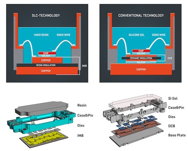
Figure 5: Comparison of SLC technology and standard package technology with base plate; cross-section comparison on the top and explosion image comparison on the bottom
The IMB replaces the conventionally used ceramic isolation DCB and combines an electrically insulating resin layer with a directly bonded top- and bottom-side copper layer. Careful selection of the insulation material and resin layer thickness ensures the required insulation and heat dissipation properties. The insulating resin layer has the same coefficient thermal expansion (CTE) value of about 17x10-6/K as the copper layer. As a result, the thermomechanical stress caused by any mismatch between two different CTEs has been reduced. Furthermore, the baseplate solder layer is completely eliminated as the top and bottom copper layers are directly bonded to the insulating resin layer.
As a result, the thermal cycling capability of the SLC technology is superior and ongoing results show a significant improvement in thermal cycling capability when compared to standard package technology. Finally, as mechanical stress in the solder layer increases with substrate size, the maximum size of standard packaging technology DCBs is limited. As shown in Figure 5, two or three substrates are therefore necessary to ensure thermal cycling capability of standard packaging technology. These multiple substrates have to be electrically connected with wires which increases the internal parasitic inductance. SLC Technology does not suffer from these limitations thanks to the use of the common IMB. It also increases the effective area available for dies and gives more flexibility for optimal layouts.
The second key element of the SLC technology is the use of hard DP-resin compared with the soft silicone gel of the standard package technology. The DP-resin distributes the mechanical stress on the wire bonds more homogeneously and helps support the wire bond solder joint which improves the power cycling capability. In addition, the CTE value of the DP-resin is similar to that of the IMB and the case. This eliminates the “pumping-out” failure phenomenon where the thermal interface material is “pumped out” from the module-heat-sink interface during temperature cycling.
With the combination of the IMB and the hard DP-resin encapsulation, VINco E3 offers a high-reliability mid-power package for the industrial market.
Application Benchmark
The key features of the new M7 chip technology and the new SLC packaging technology have been described above. Every new technology should be compared with the established standard technologies and demonstrate its performance and benefits for the customer. This has been done with an application benchmark between the VINco E3 and a standard industry package from the best competition on the market. Both modules have been measured and simulation models have been created. VincotechISE[1], the simulation software used for the benchmark, provides a fast and accurate way of comparing power losses and temperatures at various operating points. The flowSIM tool simulates Vincotech power modules for industrial drive applications. It features parameter setup and function blocks tailored for industrial drive applications.
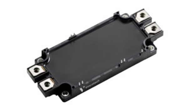
Figure 6: VINcoDUAL E3
The application benchmark compares the 1200 V/600A VINco E3 (A0-VS122PA600M7-L759F70) module with a similar module from the competition. A typical motor drive operation point has been selected for the comparison: Iout 300A, Vout 380V, cosPhi 0,8, Theatsink 80°C and the benchmark simulations use the same gate resistance value of 2Ohm for both modules. These conditions model a typical 2nd source strategy where a customer uses a single application board design on a production line but can select between different supplier power modules during manufacture depending on availability.
Figure 7 shows the total power loss simulation results for different switching frequencies. The new M7 chip technology in the VINco E3 package reduces the power losses by up to 13% compared with the competitor module. The superior dynamic performance of the M7 diodes is a major contributor to the loss reduction, but also the dynamic and static characteristics of the IGBT M7 contribute to the loss reduction. This loss reduction results in higher efficiency and contributes to the energy savings and eco-friendly operation of the inverter.
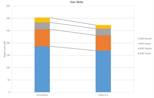
Figure 7: Total power loss simulation comparison between VINco E3 (1200 V/450 A) and appropriate competitor for a typical motor drive operation point Iout 300 A, Vout 380 V, cosPhi 0,8 and switching frequencies from 4 kHz up to 16 kHz.
VINco E3 Line-up Plan
The initial VINco E3 modules available support blocking voltages up to 1200V in a half-bridge configuration and cover current ratings from 300A to 690A. Sixpack and PIM topologies are under development as well as blocking voltage classes 650V and 1700V. To support higher current ratings and higher blocking voltages, a new IMB is in the qualification phase with an improved insulating resin layer. Table 1 shows the comprehensive VINco E3 line up currently in development featuring the new M7 chip technology and the new SLC package technology to support a wide range of application. Following a multiple source strategy to provide customers with the highest supply chain security, the new VINco E3 will also be available with additional chip technologies such as the IGBT4 Trench field. VINco E3 will also be available with press-fit terminals and pre-applied phase change material for a cost-efficient assembly process.
| Topology | Housing | VCES 650V | VCES 1200V | VCES 1700V | Chip Technology |
| Half-Bridge | VINcoDUAL E3 | 300 A | 300 A | 300 A | IGBT M7 / Trench IGBT4 |
| Half-Bridge | VINcoDUAL E3 | 450 A | 450 A | 450 A | IGBT M7 / Trench IGBT4 |
| Half-Bridge | VINcoDUAL E3 | 600 A | 600 A | 600 A | IGBT M7 / Trench IGBT4 |
| Half-Bridge | VINcoDUAL E3 | 690 A | IGBT M7 | ||
| Sixpack | VINcoDUAL E3 | 100 A | 100 A | 100 A | IGBT M7 / Trench IGBT4 |
| Sixpack | VINcoDUAL E3 | 150 A | 150 A | 150 A | IGBT M7 / Trench IGBT4 |
| Sixpack | VINcoDUAL E3 | 200 A | 200 A | IGBT M7 / Trench IGBT4 | |
| PIM | VINcoPIM E3 | 150 A | IGBT M7 / Trench IGBT4 | ||
| PIM | VINcoPIM E3 | 150 A | 100 A | IGBT M7 / Trench IGBT4 | |
| PIM | VINcoPIM E3 | 100 A | 75 A | IGBT M7 / Trench IGBT4 |
Table 1: Planned line up of the new VINco E3 product line
The new VINco E3 product line offers an efficient and reliable mid-power package by utilizing the new M7 chip technology and the SLC package technology. The new IGBT M7 offers superior performance for industrial drive applications and helps meet development goals for lower power losses, higher efficiency, and eco-friendly operation inverters. The new SLC package technology with the IMB and the hard DP-resin encapsulation provides a high-reliability package with a superior thermal cycling capability. The combination of these two features utilized in VINco E3 ensures flexible and cost-optimized inverter designs.
About the Author
Dr. Evangelos Theodossiu is the Senior Product Marketing Manager at Vincotech. He manages all new product development projects from initial concept to launch. Dr. Theodossiu has a doctorate in physics from Johann Wolfgang Goethe-Universität Frankfurt am Main.