Facebook
 Google
 GitHub
 Linkedin
Addressing the Challenges of Utilizing IGBT Technology in Power Modules
This article features Vincotech GmbH IGBTs in power modules as it getting thinner, smaller, and faster that complicates their installation in power modules.
Power semiconductors are getting thinner, smaller, and faster, and the challenges for manufacturers that employ the latest chip technology in their power modules are getting bigger.
A sure-fire way to decrease losses and increase power density is to improve switching behavior. From the perspective of a device designer seeking to boost a power-converting system’s energy efficiency, this is certainly the best choice of parameters. Power module manufacturers will have to incorporate state-of-the-art IGBT technology into the product to afford designers the option of tweaking these parameters.
The IGBT powered by Infineon TRENCHSTOP™5 H5 is designed for a 15-to-80 kHz carrier switching frequency range with a maximum blocking voltage of 650 V. Available in discrete housings such as the TO-247, it is designed for systems with a stray inductance of 30 to 50 nH for the PCB tracks. [1]
Vincotech is one manufacturer that uses these devices, rather than discrete packages, in power modules. The flow family of modules can handle IGBT’s performance. The company builds power modules with low internal stray inductance that can accommodate many different types of fast-switching power semiconductors, including this 650V chip.
Housing
The flow family’s special housing technology has enabled Vincotech to rise to the challenge of incorporating the latest chip technology in a power module with features that include:
- No baseplate
- Low internal stray inductance
- Freely positioned auxiliary pins (solder, press-fit)
- DC capacitors built into the module
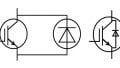
The flow 1 housing pictured in Figure 1 features very fast dies in a neutral point clamped (NPC) inverter topology. Also known as I-type topology, it is deployed in three-level converters designed mainly for solar and UPS applications. The combination of fast switching IGBTs, fast diodes, and integrated DC capacitors ensures highest efficiency and fast switching capability in a compact power module (item code 10-FY07NPA200SM02-L366F08).

Figure 1. flowNPC 1 with integrated DC capacitors, 650V IGBT, fast diodes, and a temperature sensor [2]
Measurements: The Impact of DC Capacitors
The nature of an IGBT’s design makes it all but impossible for the gate-resistor Rg to control turn-OFF behavior. The corresponding collector-emitter voltage peak (Vcep) during turn-OFF depends on the turn-OFF speed of the current and on the stray inductance L between the capacitors and the semiconductor at a given collector-emitter voltage Vce.
The equation describes the voltage overshoot ΔVcep at turn-OFF, a relationship that is very well known. This equation tells us that decreasing the stray inductance or the turn-OFF rate will reduce the voltage overshoot across the IGBT.
Figure 2 shows the integrated DC capacitors’ impact on the collector-emitter peak voltage in a power module. The measurements with an integrated DC capacitor (orange) and without it (blue) were taken under the same testing conditions.

Figure 2. Two power modules’ turn-OFF waveform at the given current Ic with an integrated DC capacitor (orange) and without (blue)
The chart clearly indicates that without an integrated DC capacitor, the collector-emitter voltage Vce oscillates after a turn-OFF voltage peak of around 218% of the applied DC link voltage of 350V from neutral point to DC. The integrated DC capacitor not only reduces the Vcep to 137% of the DC link voltage; it also suppresses oscillation.
Placing a DC capacitor as close to the IGBT as possible is definitely the smart move for very fast switching power semiconductors.
Measurements
Characterizing Switching Behavior
Dynamic characteristics need to be analyzed regardless of the low inductive package design. The slopes of the collector-emitter voltage Vce and the nominal current Ic during turn-ON and turn-OFF have to be handled, particularly when using a fast IGBT. This is why the measurements focus on these switching slopes, respectively dV/dt and dI/ dt of the T3 (Figure 1). Slowing down power semiconductor’s switching speed decreases the switching slopes, thereby increasing power loss.
Figure 3 shows the turn-ON current slope dI/dt_on (solid lines) and the reverse recovery dI/dt_rec (dashed lines) behavior in accordance with the gate resistance Rgat room temperature (blue) and 125°C (orange).

Figure 3. Turn-ON dI/dt at 25°C (blue) and 125°C (orange). Reverse recovery dI/dt at 25°C (black) and 125°C (orange).
Values below 4Ω are not shown because of measurement noise.
The turn-ON speed at 25°C drops from 4Ω onwards down to around 45% of the peak value at 16Ω. Temperature has a slight but discernible impact on the turn-ON current slope, as the dI/dt_on values at 125°C attest: They remain below values measured at 25°C. The turn-ON speed’s reduction from the peak to the lowest value at 125°C amounts to around 47%.
Figure 3 also shows the reverse recovery current slope dI/dt_rec; that is, the curve’s post-peak current trajectory. Temperature has very little impact; the curves are very similar and practically identical at around 7Ω.
Figure 4 shows collector-emitter voltage switching slopes in relation to Rg. The turn-OFF voltage slope remains fairly constant above 4Ω, which confirms that the physics of semiconductors are such that turn-OFF behavior can hardly be controlled by Rg. The turn-OFF dV/dt is quite stable throughout gate resistance range; the only discernible impact is to be seen at turn-ON.
At low Rg, dV/dt_on is high. A higher resistance value can bring it down. The turn-ON behaviors at 25°C and 125°C (solid lines) are similar. The only difference would appear to be the turn-on dV/dt reduction that subsequently occurs at 25°C.

Figure 4. Turn-ON (solid lines) and turn-OFF (dashes) dV/dt at 25°C (blue) and 125°C (orange)
Figure 5 depicts turn-ON and turn-OFF switching energies. The solid lines represent measurements of turn-OFF energy Eoff; the dashes show the data for turn-on and reverse recovery energy (Eon and Err) at room temperature and 125°C. These readings were taken to investigate to what extent Eon, Eoff, and Err depend on Rg. Eon, Eoff, and Err similar tendencies at both temperatures.

Figure 5. Switching energies of T13 in relation to Rg at 25°C and 125°C. This graph shows Eoff (solid lines), Eon and Err (dashes lines).
The inset graph shows the total energy at 25°C (blue) and 125°C (orange).
Eon increases with increasing gate resistance because the IGBT slows down and device loss increase. Consequently, reverse recovery energy decreases slightly because of a lower reverse recovery peak, which is in accordance with the dI/dt_rec behavior to be seen in Figure 3.
In terms of the dI/dt steepness and given the total energy Etot at 25°C (blue) and at 125°C (orange) as shown in Figure 5’s inset graph, a gate resistor with more than 4Ω would appear to be a reasonable proposition. However, this would require a tradeoff between the current slopes and total energy losses because of the loss that increases with increasing gate resistance. As we have seen in Figure 4, the gate resistance has hardly any impact on the turn-OFF dV/dt or on Eoff.
IGBTs in Power Modules
IGBTs are getting faster, which complicates their installation in power modules. Integrated DC capacitors can be very beneficial to this end as they prevent turn-OFF voltage overshoots. We measured a reduction from 218% to 137%.
Furthermore, designers also have to strike the right balance between switching speed, switching loss and dV/dt-controlled electromagnetic compatibility for the power-converting system. Our measurements tell us that they need to choose the right gate resistor to this end. In this case, a resistance value greater than 4 ohms would appear to be the best choice for a tradeoff between total energy loss and switching slopes. However, every system and application is different and the right Rgvalue for each has to be determined with the proper measurements.
About the Author
Daniel Hofmann is an EMEA field applications engineer for Vincotech GmbH in Frankfurt, Germany. He graduated from Johann Wolfgang Goethe-Universität Franfurt am Main in 2011 with a degree in physics and has been working in the electronic engineering sphere since then.
References
- Infineon, Application Note AN2015-15 Rev. 1.0, TRENCHSTOP™5 S5 Infineon’s low Vce(sat) high-speed soft-switching IGBT
- Datasheet of 10-FY07NPA200SM02-L366F08, Vincotech
This article originally appeared in the Bodo’s Power Systems magazine.