Facebook
 Google
 GitHub
 Linkedin
The Efficiency Revolution: Migrating to Advanced Low-Standby Power Architectures
This article discusses the optimization of advancing to low-standby power architectures.
The power electronics industry has come a long way in the last 30 years and the pace of development shows no signs of stopping. In the area of technology advances, the numbers for operational efficiency keep going up, to the point where some Point-of-Load (PoL) and other board-level devices are exhibiting efficiency numbers approaching the theoretical maximum.
How do you save energy in a power supply that’s already 95%+ efficient? One answer is to reduce the amount of energy a device consumes when it is in standby mode. This ‘vampire’ power usage has been an issue for years, first manifesting itself in the first generation of remote-controlled, ‘instant-on’, power-hungry television sets. Some consumers would unplug the sets when not in use to reduce their household energy bills (arguably, this is the first example of zero quiescent power, albeit under direct human control).
Once standby power was recognized as a serious area for energy conservation (think of the millions of unused phone chargers plugged into walls at this very moment), governments began to issue regulations on the matter. From ENERGY STAR to the Federal Energy Management Program to the EU’s ErP (Energy Related Products) Directive, there has been a tremendous pressure to both increase efficiency while reducing standby power, a trend that has all-but-eliminated the use of linear power supplies in some markets.
Such regulatory requirements for standby, ‘off’, and networked standby performance in power consumption in electrical and electronic household and office equipment are forcing the power electronics industry to migrate systems to the next level. In the case of the ErP, the commission is looking to further improve low-load efficiency significantly (see Figure 1). The most recent study was completed in April 2017, with likely implementation in 2021. Since January 2017 networked standby devices must not consume more than 3 to 8 watts depending on the product, compared to 20 to 80 watts previously.
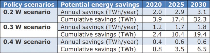
Figure 1: The ErP commission is looking to further improve low-load efficiency.
Standing By
Any intelligent device that needs to immediately respond to input must draw power to operate, even if momentarily on a long duty cycle. Generally, the touch-screen and/or user interface and/or wireless connections may remain on in rest states, requiring enough power to keep them alive, while still achieving the standby requirement. This demands high-efficiency operation at light loads, among other things.
One way to address this need is with Power Integrations’ InnoSwitch™ technology, with ON/OFF control to maximize efficiency at light load. In addition to having the most efficient algorithm in low power, this functionality enables the device to only deliver power when output is needed. InnoSwitch-based devices always switch at the minimum frequency possible, reducing switch losses that kill efficiency at light load. In addition, InnoSwitch also provides excellent cross-regulation in multi-output designs, eliminating the linear regulator for secondary outputs that hurts efficiency at light load. Synchronous rectification also allows an efficiency increase by several points in standby. The InnoSwitch-EP architecture is revolutionary in that the devices incorporate both primary and secondary controllers, with sense elements and a safety-rated feedback mechanism into a single IC (Figure 2). PSR (primary side regulators) can only measure output voltage when they are switching. But when they are switching they are sending energy. If too much energy gets sent just for checking’ the output voltage, then it needs to be burned or the output voltage will ratchet up. This forces PSR based units to trade off speed-of-response with no-load energy use. However, because the InnoSwitch architecture does not require a pre-load, it is naturally ‘low-load’ and also very fast.
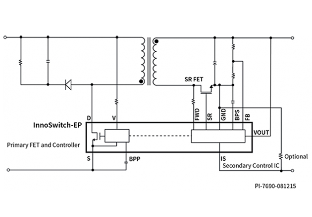
Figure 2: The InnoSwitch-EP flyback switcher IC in a typical application.
Close component proximity and innovative use of the integrated communication link permit accurate control of a secondary-side synchronous rectification MOSFET and optimization of primary-side switching to maintain high efficiency across the entire load range. Additionally, the minimal DC bias requirements of the link enable the system to achieve less than 10 mW no-load to maximize efficiency in standby.
Optimize Your Design
Design optimization is fundamental to reach the highest level of efficiency available to a system. A power circuit in one sense is a chain that is only as efficient as the weakest link in it. An improvement in one portion of design may result in some improvement, but if every point in the circuit is optimized, much more significant results will be realized.
Figure 3 shows the levels of efficiency achieved by using the best solution at each point in the chain. In this case, a non-isolated flyback converter was created that provides a dual output of 5 V at 650 mA and 12mV at 400 mA from input from 85 VAC to 350 VAC. This power supply utilizes the LNK3696P from the LinkSwitch™-XT2 900 V family of devices, which is optimized for industrial and metering applications operating off voltages up to 480 VAC.
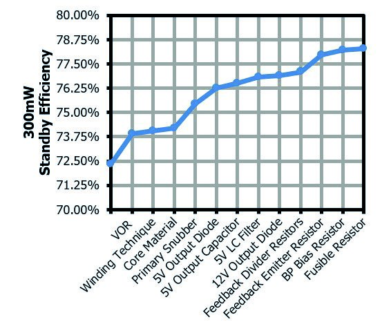
Figure 3: The levels of efficiency achieved by using the best solution at each point in the chain.
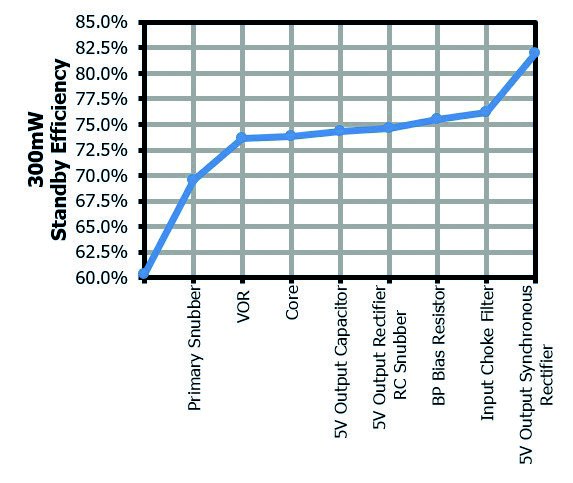
Figure 4: Design optimization in a 15 W dual-output converter based on the InnoSwitch3-EP.
The accurate design-in of each component adds another six points of efficiency at 300 mW, underscoring the importance of total system optimization. A clampless design can be used in low-power applications to further improve efficiency. Note how each step in the optimization chain adds its own contribution to overall system efficiency.
Another example can be found in Figure 4, showing the improvement that design optimization can provide in a 15 W dual-output (5 V/1.2 A and 12 V/0.75 A) converter based on the InnoSwitch3-EP. The design achieves greater than 83% standby mode efficiency and is ErP compliant. Just like the previous example, design optimization of Vor and primary snubber are important.
This design improves standby efficiency by maximizing the available output power for any given input power, with an optimized transformer design along with the best selection of active devices, primary clamp, filter components, and bias resistors. For 15 W the design can use a clampless approach, but the transformer design is more complicated. In addition, synchronous rectification (SR) can give a big boost in efficiency versus a conventional output.
Looking Forward
These advances in power electronics provide many benefits beyond the obvious ones. The biggest advantage is in the reduced bill of materials that results in using an optimized integrated design. If you compare the costs of a linear power supply from 10 years ago to the cost of a modern switcher based on technologies like InnoSwitch, the new supply is significantly less expensive in quantity. Even more significant differences can be found in the reduced size, weight, and thermal requirements of the modern power solution. These advances provide cascading benefits across the board, from smaller form factors and higher thermal efficiency to lower BoM costs due to reduced component counts.
To address requirements like the new EuP, the latest core technologies must be employed, as well as an optimal system design for the best possible efficiency and performance. Using innovative technologies like InnoSwitch, with ON/OFF functionality, integrated SR, and its highly-efficient algorithm, designers can enjoy real benefits and deliver the best power solution for their application.
Dynamic Configuration Enables Precise Control
Capable of delivering up to 65 W and achieving up to 94% efficiency across line and load conditions, the InnoSwitch3-Pro family of off-line CV/CC and CP flyback switcher ICs enable precise, dynamically adjustable, control of voltage (10 mV step) and current (50 mA step), via a simple two-wire I2C interface. Devices may be paired with a microcontroller or take inputs from the system CPU to control and monitor the off-line power supply. Applications include virtually any rapid-charging protocol, including USB Power Delivery (PD) 3.0 + PPS, Quick Charge™ 4/4+, AFC, VOOC, SCP, FCP and other industrial and consumer battery chargers, dimmable LED ballast drivers and field-configurable industrial power supplies.
A microprocessor VCC supply is included, eliminating the need for an external LDO to power the microcontroller; also included is an n-channel FET driver which may be used to enable or disable the main power output. Together with integrated bus voltage, current and fault-reporting telemetry and dynamically configurable protection functions such as OTP, line OV/UV, output OV/UV, and short-circuit, the BOM count for a sophisticated offline power supply is significantly reduced and design complexity is considerably simplified.
This combination of features addresses current market challenges as the AC-DC power conversion market rapidly-transitions with system designers needing a programmable solution that can adapt to various fast-charging protocols including the recently completed USB PD 3.0+ PPS specification. The ability to precisely control the output voltage and current of a power supply over a wide range is also useful for designers of specialized applications with smaller production runs, as they can easily configure a single board design for multiple product SKUs using software either at manufacture or during installation.
InnoSwitch3-Pro ICs employ Power Integrations’ high-speed digital communications technology, FluxLink™, plus synchronous rectification, quasi-resonant switching and precise secondary-side feedback sensing and the feedback control circuit. Devices are CQC certified, UL recognized and TUV (EN60950) approved to bridge the isolation barrier; the products’ InSOP™-24D package also provides a low-profile, thermally efficient solution with extended creepage (>11.5 mm) and the clearance between primary and secondary sides for high reliability, surge protection, and ESD robustness.
About the Author
Silvestro Fimiani is a Product Marketing Manager at Power Integration for more than 13 years. He got his bachelor’s degree in Physics at the University of Naples Federico II and after his education, he got a lot of experience in different companies with various job positions that are related to electronics.
This article originally appeared in the Bodo’s Power Systems magazine.