Facebook
 Google
 GitHub
 Linkedin
New Silicon Anode Architecture Could Give New, Extended Life to Lithium-Ion Batteries
Lithium-Ion batteries (LIBs) are highly important to the ever-evolving electronic market, powering systems from cellphones and laptops, all the way to Electric Vehicles (EVs). With this in mind, every effort to make LIBs more efficient, longer lasting and higher performing is being made, and a team at the Okinawa Institute of Science and Technology Graduate University (OIST) is doing just that.
New research from OIST claims finding a new building block improving the anodes of LIBs according to a press article from the school. The team specifically has moved from the traditional graphite anode to a nanostructure of silicon.
This change is due to the science behind the operation of LIBs. During the charging process, lithium ions travel from the cathode of the battery, through an electrolytic solution, to the anode, and they move in the reverse direction during normal operation. In order to maximize these processes, the anode must be able to store as many lithium ions as possible. The more it stores, the higher the battery’s charge density, and longer its cycle lifetime. Graphite is not ideal for this, as it takes six carbon atoms (the building block of graphite) to store a single lithium ion. Now for silicon, a single atom can store four lithium ions, a huge increase in energy density implications.
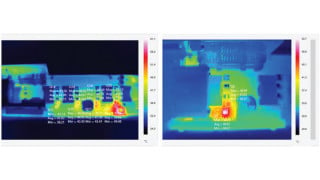
While the shift to silicon seems obvious, many have stayed away from it for structural integrity reasons. When the charges move into the anode, there is a huge volume change, around 400% according to Dr. Marta Haro, a former researcher at OIST. This can cause a silicon anode to fracture and break, and a protective layer that usually develops between the electrolyte and anode while the battery is being charged, would not effectively form due to the volume change. This too will affect battery performance, more over the long haul as it will reduce lifespan and rechargeability.
To fight these concerns, the team worked to extend the findings of a previous research paper that discovered creating a cake-like layered structure of silicon sandwiched between tantalum metal nanoparticles. This nanostructure is made using the method shown in the figure below:

Figure 1: In chamber 1, the nanoparticles, made from tantalum metal, are grown. Within this chamber, individual tantalum atoms clump together, similar to the formation of rain droplets. In chamber 2, the nanoparticles are mass filtered, removing ones that are too large or too small. In chamber 3, a layer of nanoparticles is deposited. This layer is then “sprayed” with isolated silicon atoms, forming a silicon layer. This process can then be repeated to create a multi-layered structure. Image Courtesy of OIST.
They found, through microscopy and computer simulations, that when they gradually made the silicon layer thicker, the material would become gradually stiffer, as expected, but at one specific point, would begin to greatly decrease in stiffness as the thickness continued to be increased.
They found that this spike in stiffness was due to the fact that as more silicon atoms are deposited onto the nanoparticle layer, they begin to create columns in the shape of inverted cones, not uniform films as one would expect. These cones then will grow to touch each other, forming a vault structure, much like a civil engineering arch in civil engineering according to Dr. Grammatikopoulos, senior author of the paper.
If more silicon atoms are deposited once this arch is made, it will create pores within the structure and it will become very weak, acting as a sponge, so there is a very precise moment when the structure of the silicon anode is maximized for stability. The stages of the silicon structure based on the thickness of the layer is shown in the below figure.

Figure 2: In the first stage, the silicon film exists as a rigid but wobbly columnar structure. In the second stage, the columns touch at the top, forming a vaulted structure, which is strong due to arch action. In the third stage, further deposition of silicon atoms results in a sponge-like structure. The red dashed lines show how the silicon deforms as a force is applied. Image Courtesy of OIST.
Importantly, the same silicon thickness that gives maximum stability also gives the best electrochemical characteristics for the battery. The protective layer also was seen to be more stable with the silicon anode constructed in this way, so overall this silicon nanostructure seems to solve all the issues that come with making a silicon anode, while providing all of the benefits.
We’ve seen that this material advancement can benefit the LIB industry, but the team says that this is just the beginning. Dr. Grammatikopoulos talks about how these materials can be used in other applications that require strong nanostructures that can withstand varying degrees of stress, like in bio-implants and the storing of hydrogen, and the method can be used to create materials that are just as strong or weak, and flexible or rigid as you would like.
“That’s the beauty of nanostructures.” Dr. Grammatikopoulos said.