Facebook
 Google
 GitHub
 Linkedin
IEDM to Feature Gallium-Nitride Power Semis & ICs and Thin-Film Solid State Batteries
Among the power electronics related papers at the 65th IEEE International Electron Devices Meeting (IEDM), to be hosted in San Francisco from 7 to 11 of December, will be advances in thin-film solid state batteries, 1200V gallium-nitride (GaN) power devices and monolithically integrated GaN-on-SOI ICs for power conversion.
CEA-Leti researchers will discuss a thin-film battery with the highest areal energy density yet reported (the graph above summarizes the results of this study and compares them with previous efforts). A team led by EPFL will report on novel lateral multi-channel AlGaN/GaN power devices with high breakdown voltage (1230V) and low on-resistance (2.8Ω⋅mm), resulting in an excellent figure-of-merit of 3.2GW/cm2. And a team led by imec will discuss monolithically integrated GaN-on-SOI ICs for power conversion, which they used to build a complete buck converter that demonstrated 200V on-chip power conversion at 1MHz.
Outstanding GaN-on-Si Performance:
Lateral GaN-on-Si devices are promising for advanced power ICs because they combine high device performance, low cost, and can make physically smaller systems possible. While GaN HEMTs are commercially available, there is still plenty of room to improve their performance up to the full potential of GaN, and further advances require a major advance in on-resistance while still maintaining high breakdown voltage.
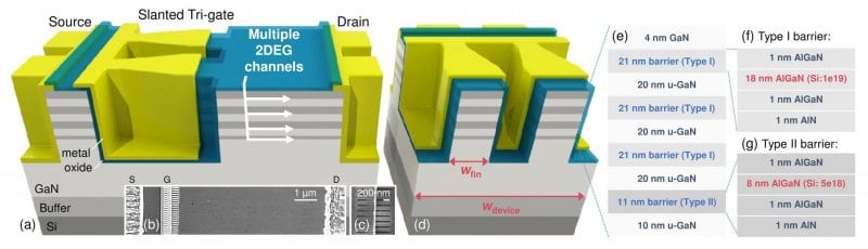
A team led by EPFL will report on novel lateral multi-channel AlGaN/GaN power devices with high breakdown voltage (1230V) and low on-resistance (2.8Ω⋅mm), resulting in an excellent figure-of-merit of 3.2GW/cm2.
The researchers call these devices MOSHEMTs, and they have a multi-channel FinFET-like architecture with slanted tri-gates whose structure can be modified to "tune" device performance. The on-resistance is some 5x lower than previously seen at this breakdown voltage with single-channel devices. Until now it has proven difficult to control multiple parallel channels with a typical gate architecture, but the tri-gate structure has proven to be effective in doing so, and it lends itself to building normally-off - and thus more fail-safe - devices.
 (click on image to enlarge)
 (click on image to enlarge)
In the schematic above, (a) shows the multichannel slanted tri-gate MOSHEMTs, (b) is a top view, (c) are zoomed SEM images, (d) is a cross-sectional schematic of the devices, and (e-g) illustrate the four-channel structure which contains four parallel multi-channels formed by two types of barrier layers. The plots below it benchmark the slanted tri-gate MOSHEMTs against conventional single-channel GaN-based HEMTs, showing substantial improvements in on-resistance (left) and breakdown voltage (right).
(Paper 4.1, "1200 V Multi-Channel Power Devices with 2.8 Ω⋅mm ON-Resistance," J. Ma et al., EPFL/Enkris Semiconductor)
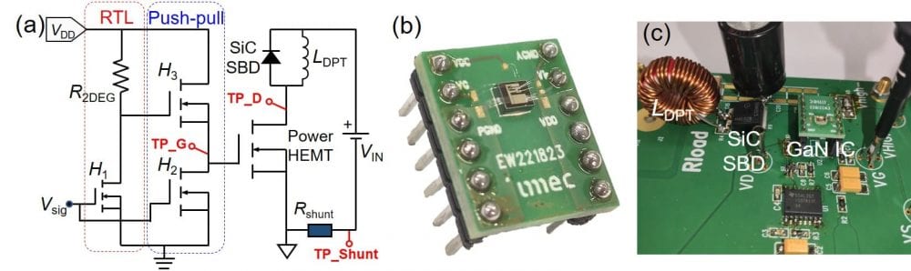
Monolithically Integrated GaN-on-SOI Platform Technology:
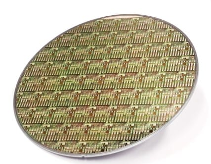
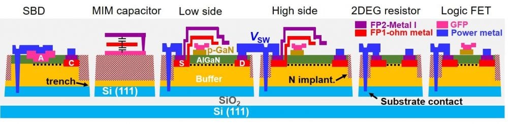
A team led by imec will discuss monolithically integrated GaN-on-SOI ICs for power conversion, which they used to build a complete buck converter that demonstrated 200 V on-chip power conversion at 1 MHz. An SOI (silicon-on-insulator) substrate was used because it eliminates the back-gating effect which wastes power. It also suppresses parasitics, provides effective electrical isolation and reduces the area required.
The team comprehensively investigated the technology from multiple vantage points: substrate, buffer, isolation, device, co-integration and circuit. Different components were successfully integrated monolithically, including a HEMT, Schottky barrier diode, MIM capacitor, 2DEG resistor, and resistor-transistor logic.
 (click on image to enlarge)
 (click on image to enlarge)
The upper image is a photograph of the processed GaN ICs on a 200mm GaN-on-SOI substrate. The schematic in the middle shows process cross-sections of the GaN IC components on GaN-on-SOI substrate. Below is (a) a schematic of a double-pulse test circuit, (b) packaging of the GaN IC with an integrated driver and power HEMT, and (c) printed circuit board.
(Paper 4.4, "GaN-on-SOI: Monolithically Integrated All-GaN ICs for Power Conversion," X. Li et al., Imec/KU Leuven)
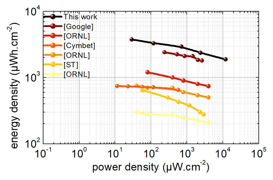
High Energy-Density Thin-Film Battery:
There has been great progress in miniaturizing electronics but the miniaturization of power sources hasn't kept pace. Although integrated electrochemical capacitors offer high power density, high frequency response and novel form factors, their low energy densities are of limited value for MEMS and autonomous device applications that require long periods between charging. CEA-Leti researchers will discuss a thin-film battery (TFB) with the highest areal energy density yet reported (890µAh/cm-2) and high power density (450µAh/cm-2).
Built on silicon wafers using UV photolithography and etching for the successive deposition and patterning of each layer, the thin-film battery integrates a 20µm-thick LiCoO2 cathode in a Li-free anode configuration. It showed good cycling behavior over 100 cycles, and the fact it was built using a wafer-level process opens up the possibility to tightly integrate this battery technology with future electronic devices.
 (click on image to enlarge)
 (click on image to enlarge)
The top images show SEM cross-sectional characterizations of (a) sub-100µm-thick TFB structure and (b) active layers. The graph below summarizes the results of the study and compares them to previous work. It shows that these TFBs exhibit the highest energy and power densities yet reported.
(Paper 26.1, "Millimeter-Scale Thin-Film Batteries for Integrated High Energy-Density Storage," S. Oukassi et al., CEA-Leti)