Facebook
 Google
 GitHub
 Linkedin
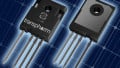
Diamond-Based WBG Semis to Ship in Q1 2016
AKHAN Semiconductor, Inc. is celebrating the opening of its new global headquarters and production facility in Gurnee, Illinois, and announcing that its first commercial customer will take delivery of the first AKHAN diamond semiconductor based-technology products in Q1 2016. The opening of the AKHAN production facility marks a major milestone for AKHAN Semiconductor and is the culmination of a decade of development and collaboration. AKHAN is actively hiring to staff the new facility which is expected to employee 100 people in the next two years.
Diamond is a wide bandgap (WBG) material. Its ability to conduct heat far surpasses that of materials used on current electronics (five times better than copper, 22 times better than silicon). It also has the unique ability to isolate massive voltages with a small fraction of the material required compared to present technologies. In isolating 10,000V, the amount of diamond needed is 50 times less than that of silicon.
The company's comprehensive Miraj Diamond™ platform is at the center of AKHAN Semi’s ability to manufacture next generation diamond semiconductor technology. The platform enables fabrication of complex devices such as high speed/power transistors, RF, and microwave electronics. The product offering within this platform consists of both passive and active semiconductor material and component device systems. The technical feasibility, process development, and device fabrication, prior to full commercialization, has been completed utilizing wafer fabrication centers at several locations in the US.
Considering diamond’s status as a luxury material to most, the idea of integrating it with electronics may appear costly. AKHAN Semi has overcome this hurdle by developing a state-of-the-art manufacturing process that takes common methane gas as the input, and produces the perfect diamond wafers needed for electronic production. At a basic level, the process is to crack the methane gas onto a heated platform using a ball of plasma. This process occurs inside of an MPCVD reactor. The final product is a diamond wafer which can be used as a platform for fabricating the semiconductor devices.
AKHAN’s technology is based on a new process that uses man-made diamond rather than silicon to produce new chip materials that are more cost effective, operate at higher temperatures, are thinner and require less power. It is a result of the marriage of two scientific breakthroughs: ability to use nanocrystalline diamond (NCD) films and a new doping process the makes it possible to use NCD as a semiconductor material.
“As a native of Gurnee, I am proud to help spur a new era of innovation and semiconductor technology in my hometown, in the state of Illinois, right here in the Diamond Prairie,†said Adam Khan, CEO and Founder of AKHAN Semiconductor. “The opening of our new global headquarters and production facility is just the first step in our goal to transform the chip industry and to extend Moore’s Law. Our diamond semiconductor based technology will enable a new generation of commercial, industrial and consumer products such as flexible and transparent displays that can be used in wearables and thinner consumer devices that last longer. On the commercial side, we expect to develop new products such as diamond windows for industrial, defense and aerospace applications.â€