Facebook
 Google
 GitHub
 Linkedin
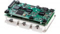
750W Digital ZVS-FB AC-DC Reference Design with Semi-Bridgeless PFC
Microchip's 750W ac-dc reference design demonstrates a semi-bridgeless PFC topology followed by a peak current controlled zero-voltage switching full-bridge (ZVS-FB) converter with digital slope compensation to achieve very high conversion efficiencies. This power supply can be firmware updated (including the compensator algorithm) with zero down time to the system it is powering while the power supply is running.
It is implemented using two dsPIC33EP "GS" digital-power DSCs that provide full digital control of the power conversion as well as all system management functions.
The ZVS-FB converter is designed to stepdown an input dc voltage of 400V to an output dc voltage of 12V. A unique feature of the reference design is the implementation of peak current control, using a fully software-based slope compensation algorithm, which eliminates the use of external analog components for slope compensation.
The 750W ac-dc reference design is royalty free when used in accordance with the licensing agreement. Features of this reference design include:
- Full digital control
- Standardized form factor: 1U
- 20ms minimum hold-up time to compensate drop-outs during UPS step-in
- Under/Over voltage lock-out
- Adaptive control
- Peak current controlled ZVS Full Bridge Converter with unique adaptive digital slope compensation software
- Demonstration of Online Firmware updates (Live Update) on both PFC and dc-dc converter stages
Background
There is a growing need for higher efficiency, reliability and power density across the power electronics industry. These needs have driven the rapid growth of digital power solutions, especially in telecom and server power areas. The advantages and challenges of digitally controlled power supplies have been a topic of discussion and debate for several years.
Integration of advanced peripherals for power supply control in microcontrollers, coupled with advanced high-speed devices in the power semiconductor industry, have led to an increased market penetration of digital power in the industry. Control techniques that were earlier the forte of analog solutions are now more feasible in the digital space.
ZVS FULL-BRIDGE CONVERTER
In this context, this reference design features the implementation of peak current control in a ZVS Full-Bridge topology (a high-level representation is shown in Figure 1), using a fully digital slope compensation technique with minimum software overhead.
 (click on image to enlarge)
In this reference design, the proposed algorithm is a patented proprietary of Microchip Technology Inc., which offers minimum software latency in its computation of the slope compensated peak current reference on a cycle-by-cycle basis.
The ZVS-FB Converter is one of the most commonly used topologies in server and telecom power supplies, battery chargers and renewable applications, mainly due to its high-efficiency operation and ease of control.
In this topology, both average current-mode control and voltage mode control implementations typically require a capacitor in series with the transformer to prevent flux walking. The peak current control implementation eliminates the need for the series capacitor by virtue of dynamic flux balancing.
PEAK CURRENT CONTROL - ANALOG
In peak current control, however, to overcome the well-known subharmonic oscillations for duty cycles larger than 50%, a slope compensation ramp is either added to the inductor current or subtracted from the peak current reference generated by the voltage loop compensator.
Peak current control is typically an analog technique, implemented using linear amplifiers, transistors, RC networks and analog comparators (Figure 2), or by using dedicated Application-Specific Integrated Circuits.
 (click on image to enlarge)
Peak current control can also be accomplished digitally in three ways. The first method is popularly called predictive peak current control. In this technique, a leading-edge modulation of the pwm is used and the duty cycle is computed at the beginning of every cycle.
This technique eliminates the need for slope compensation and an analog comparator. Here, the effective duty cycle is calculated based on the inductance, sensed input and output voltages, and the switching period. The disadvantage of this method is the dependence on the inductance value, which is susceptible to variation.
PEAK CURRENT CONTROL - DIGITAL
The second method is essentially a hybrid technique, involving a digital compensator, analog slope compensation (external), and an analog comparator (internal to the microcontroller). The hybrid technique consists of removing the analog compensator in Figure 2 and replacing it with a digital compensator. The output of the compensator feeds a "digital peak current reference" to the Digital-to-Analog Converter (DAC) of a built-in high-speed analog comparator, as shown in Figure 3.
 (click on image to enlarge)
The (internal) analog comparator then compares the DAC output to the slope compensated inductor current waveform and provides the truncation signal to the pwm module. The inductor/switch current waveform is added to a slope compensation ramp using an external analog circuitry. In addition to requiring additional components, the analog slope compensation could be suboptimal for a wide input voltage range.
The third method which is used in this reference design is a fully digital implementation, requiring no external components for implementing peak current control (a high-level representation is shown in Figure 3). The digital compensator, slope compensation and analog comparator are internal to the microcontroller. Here, the slope compensation is accomplished by an algorithm implemented in firmware.
This algorithm takes the input voltage, output voltage, inductor current and the digital peak current reference (from the digital compensator), and produces a slope compensated peak current reference, as shown in Figure 3.
The slope compensated peak current reference is then fed to the DAC of the internal high-speed comparator (inverting input). The inductor current feedback is fed directly to the non-inverting input of the comparator. The advantages of this method are better reliability due to reduced components and the ability to implement adaptive algorithms for better dynamic response.