Facebook
 Google
 GitHub
 Linkedin
130nm Platform Features High-Performance, Low-Power and Low-Cost Structured Array
Toshiba Electronic Devices & Storage Corporation today announced a new 130nm manufacturing process node based FFSA™ (Fit Fast Structured Array), an innovative custom SoC development platform featuring high performance, low cost and low power consumption.
Toshiba provides ASIC (Application Specific IC) and FFSA™ platforms that suit the customer's business environment and requirements, that also deliver efficient solutions for custom SoC development. FFSA™ devices use a silicon-based master slice which is common in combination with upper metal layers that are reserved for customization.
By customizing only a few masks, FFSA™ offers much lower NRE costs than individual ASIC development. It also enables significant reductions in development cost and provides samples and mass-production in a short period of time than for conventional ASIC's.
Additionally, FFSA™ enables higher performance and lower power consumption than FPGA (Field Programmable Gate Array) using ASIC design methodology and its library.
The 130nm process series joins Toshiba's current 28nm, 40nm, and 65nm process portfolio making FFSA™ a suitable option for the growing industrial equipment market.
The 130nm FFSA™ devices designed on the platform will be manufactured by Japan Semiconductor, a subsidiary of Toshiba Electronic Devices & Storage Corporation with a long and proven history of expertise in manufacturing ASIC, ASSP and microcomputers. This will ensure long-term supply and meet the needs of customer business continuity plans.
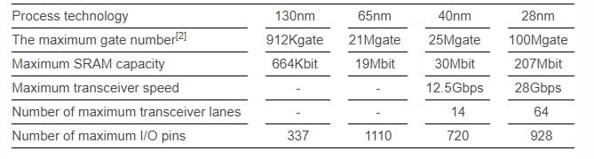 Toshiba's FFSA™ lineup
The new series deliver the performance and integration needed for industrial apparatus, communication facilities, OA equipment and consumer products where steady market expansion is expected.