Facebook
 Google
 GitHub
 Linkedin
STMicroelectronics Adds 45W and 150W Versions to its 650V MasterGaN Line
Both devices include both the gate driver and two enhancement-mode GaN power transistors in a single highly integrated package.
STMicroelectronics’ (ST) MasterGaN3 and MasterGaN5 both include two 650V eGaN power transistors with specifically designed and interfaced gate driver circuitry. This eliminates some of the serious design hurdles that might otherwise hamper the adaption of wide-bandgap, gallium nitride (GaN) technology. GaN transistors allow for more efficient designs, and they can be switched at far faster speeds than even silicon carbide (SiC) devices, let alone last-generation silicon devices, resulting in highly efficient power supplies that are as much as 80% smaller than their silicon-based antecedents.

The MasterGaN Family. Image courtesy of ST
The MasterGaN Family
The 45 watt MasterGaN3 and the 150 watt MasterGaN5 are the latest additions to ST’s group of power packages utilizing 650-volt GaN power transistors operating in half-bridg configurations. We have previously covered
- MasterGaN4, which operates at 200 watts
- MasterGaN1, operating at 400 watts
Major Highlights
MasterGaN3 devices sport GaN power transistors featuring asymmetrical RDS(ON)s of 225mΩ and 450mΩ for low side and high side respectively, making this device a good choice for soft-switching and active-rectification converters. Maximum IDS is 6.5 amps for the low side, and 4 amps for high side.
In contrast, the symmetrical MasterGaN5 power transistors are specced for 450mΩ RDS(ON)s, suiting them for deployment to active clamp flyback and LLC-resonant topologies. Maximum IDS is 4 amps.
As is the case in of all MasterGaN family members, the MasterGaN3 and the MasterGaN5 can accept input logic signals ranging from 3.3V to 15V. This makes it possible for them to be directly linked to Hall sensor outputs, MCUs, DSPs or FPGA’s.
They also implement the protections designers expect. These include undervoltage lockout (UVLO) for both high-side and low-side, over-temperature protection, gate-driver interlocks, and over-temperature protection. A shutdown pin is also provided.
Comparisons Between the MasterGaN3 and the MasterGaN5
| MASTERGAN3 | MASTERGAN5 | |
| Absolute maximum drain-to-source voltage | 620 volts | 620 volts |
| Logic power supply | 4.75V min to 9.5V max | 4.75V min to 9.5V max |
| Logic input voltage range | 0 to 20V | 0 to 20V |
| Half-bridge output slew rate (10% to 90%) | 100 V/ns | 100 V/ns |
| Thermal resistance between junction and exposed pad | 4.7 °C/W (typ) | |
| Thermal resistance low side junction to SENSE exposed pad | 2.8 °C/W (typ | |
| Thermal resistance high side junction to OUT exposed pad | 4.7 °C/W (typ) | |
| Thermal resistance junction-to-ambient | 18.8 °C/W | 18.8 °C/W |
Complete specifications can be found at the MasterGaN3 datasheet and the MasterGaN5 datasheet.
Physical Considerations
- The MASTERGAN3 and the MASTERGAN5 both operate in the -40°C to 125°C industrial temperature range.
- Both devices are available in 9 x 9 mm QFN packages.
Getting to Market Faster
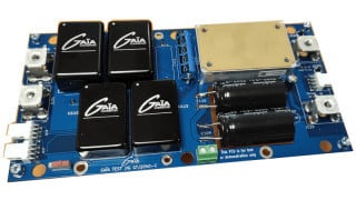
The EVALMASTERGAN3 and EVALMASTERGAN5 boards are available for the MASTERGAN3 and the MASTERGAN5, respectively. They are purposed to aid designers in understanding and evaluating the characteristics of the new power packages.

The EVALMASTERGAN5. Image courtesy of ST
These boards will also enable engineers to explore new power design possibilities without the need to design and build a completely new PCB during the early design stages.