Facebook
 Google
 GitHub
 Linkedin
STMicroelectronics Debuts MasterGaN4 for 200W Power Applications
The new power package integrates two 650V GaN power transistors with optimized gate drivers and circuit protection.
The MasterGaN4 is the latest member of ST’s popular MasterGaN family, which share the common goal to make life simpler for engineers designing power conversions applications of up to 200 watts. In one tiny, highly integrated package, ST provides the two symmetrical gallium nitride (GaN) transistors, their gate drivers and the interface circuitry, freeing up untold hours of circuit design. The units accept signal inputs over a 3.3 to 15 volt range, enabling them to directly interface with CMOS devices such as DSPs, FPGAs, MCUs or Hall-effect sensors.

Image courtesy of STMicroelectronics
The MASTERGAN4 is a power system-in-package (SIP) that includes two 650 volt enhancement mode GaN power transistors in half bridge configuration. Maximum current is 6.5 amps, the RDS(ON) is 225 mΩ, and the unit features UVLO protection on both the lower and upper driving sections. This prevents operation in dangerous conditions or in conditions of low efficiency, and the interlocking function avoids cross-conduction conditions.
The Gallium Nitride Difference
One of the principal benefits of GaNs is their ability to switch at high frequencies, enabling filtering to take place using physically smaller inductors and capacitors. Additionally, increased efficiencies reduce waste heat, calling for smaller heat sinks. It all adds up to smaller, cheaper end products with smaller BOMs and greater reliability. MasterGaN4 itself is specifically suited for symmetrical half-bridge topologies and also serves well with soft-switching topologies.
Specifications
The basic block diagram of the MasterGaN4 is identical to that of the MasterGaN1, which we have previously highlighted.

Basic block diagram of the MasterGaN4. Image courtesy of Datasheet
It’s evidently a mature design, with improvements in some parameters and a decrease in price.
The MasterGaN4 features zero reverse recovery loss, and an internal bootstrap diode for the high side driver. The maximum drain current degrades to 4.6 amps at 100℃. Peak current with 50 µs pulses is 12 amps.
Absolute maximum external capacitance between GL and PGND and between GH and OUTb are both 3.9 nF, when measured at 500 kHz. Maximum half-bridge slew rate (10% to 90%) is 100 volts per nanosecond.
Thermal data:
- Thermal resistance of each transistor’s junction to the relevant exposed pad is typically 2.8 °C/W
- Thermal resistance, junction-to-ambient, is 17.8 °C/W
Driver voltages:
- VCC undervoltage turn on thresholds are 4.2, 4.5 and 4.75 volts minimum, typical and maximum, respectively
- The equivalent values for VCC turn off thresholds are 3.9, 4.2 and 4.5 volts
Applications
- Switched mode power supplies (SMPS)
- Chargers
- Power adapters
- High voltage DC/DC and DC/AC converters
- PFC converters
Physical considerations
- MasterGaN4 is available in a 9 x 9 x 1 mm GQFN package featuring over 2 mm of creepage distance
- The power package operates over the industrial temperature range of -40 to +125℃
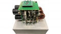
Getting to Market Faster
The EVALMASTERGAN4 is designed to help engineers to quickly evaluate the MASTERGAN4 and its characteristics. It will also allow designers to create new technologies for evaluation with no investment in hardware.

Image courtesy of EVALMASTERGAN4 Datasheet
The unit contains everything need to drive the included MASTERGAN4 with both single or complementary driving signals,