Facebook
 Google
 GitHub
 Linkedin
STMicro Unwraps GaN Power ICs for Design Flexibility
The MasterGAN6 power system-in-package integrates two 650 V GaN transistors with a high-speed gate driver, delivering 140 mΩ RDS(on), 10 A output, and low propagation delay.
STMicroelectronics has introduced the MasterGaN6, a power system-in-package that integrates two 650 V enhancement-mode GaN transistors in a half-bridge configuration with a high-frequency gate driver, housed in a 9 × 9 × 1 mm QFN package.
For engineers wrestling with ever-tighter board space and efficiency targets, the device aims to cut component count significantly while enabling switching frequencies that push the limits of what silicon can do.

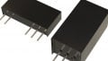
STMicroelectronics MasterGaN6 power IC.
Why GaN and Integration Matter
Power designers are constantly trying to make systems smaller and more efficient. Traditional silicon MOSFETs are reaching their practical limits in high-frequency designs. Gallium nitride (GaN) devices switch faster and reduce switching losses, allowing higher operating frequencies and giving them an edge over their silicon counterparts.
However, discrete GaN designs come with their own challenges. Fast switching increases sensitivity to parasitic inductance, and external driver circuitry can impact performance and reliability. Integrating the driver and power switches into a single package helps minimize these parasitics while simplifying PCB design.
MasterGaN6 addresses these challenges by combining GaN transistors with a high-voltage gate driver. The result is a compact and optimized power stage designed for high-frequency operation.
What’s Inside the Package
MasterGaN6 packs two enhancement-mode GaN transistors in a half-bridge configuration, each rated at a 650 V drain-source blocking voltage, with a typical on-resistance (RDS(on)) of 140 mΩ per side and a maximum continuous drain current (IDS(MAX)) of 10 A.
The device includes linear regulators on both the high and low sides of the driver to provide a stable, efficient drive voltage to the GaN switches. The high-side driver can be powered using an internal bootstrap diode, reducing the need for extra components. Turn-on resistors for both channels are externally adjustable, giving engineers direct control over switching speed to balance switching losses against EMI.
The embedded driver provides an overall propagation delay of 45 ns with a minimum pulse width of 35 ns. A short high-side wake-up time allows efficient transition from standby to active mode, enhancing burst-mode and energy-saving operation. Due to these fast switching characteristics, the IC can operate at high frequencies of up to 2 MHz in practical designs. This allows the passive components in the final design to shrink dramatically compared to silicon-based equivalents, a key reason GaN devices are smaller and lighter than their predecessors.
ST also offers several built-in protection features in the MasterGaN6 for reliable operation. Undervoltage lockout (UVLO) monitors both the main supply (VCC) and the high-side driver supply, while an interlocking function prevents both switches from turning on at the same time, avoiding cross-conduction in the half-bridge stage. The device operates over a wide temperature range of -40°C to 125°C and comes with thermal shutdown to protect against overheating.
Its input logic works from 3.3 V to 15 V, allowing it to connect directly to most microcontrollers, DSPs, or digital controllers without extra circuitry.
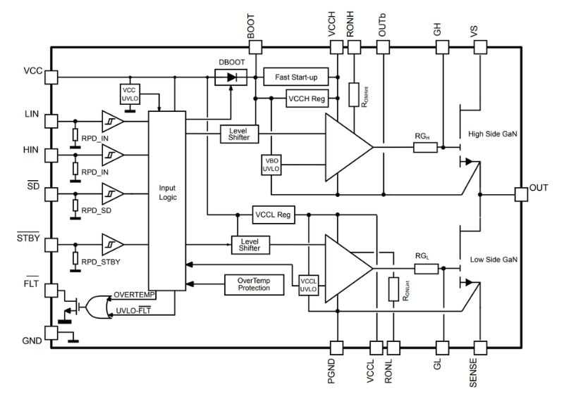
MasterGaN6 block diagram.
MasterGaN6 also includes dedicated control and status pins: STBY (standby), SD (shutdown), and FLT (fault). The standby pin places the device in a low-power state during idle periods, reducing energy consumption while allowing fast return to operation. This improves overall system efficiency, especially in applications that spend time in idle or light-load conditions.
In designs where shutdown is handled by pulling a PWM input low, the host controller must respond in software to fault conditions, a loop that may be too slow to prevent damage in a 650 V switching node. The MasterGaN6's SD pin bypasses the input logic entirely. It pulls it to GND and immediately halts switching on both the high-side and low-side transistors, regardless of the state of LIN or HIN. The FLT pin completes the picture from the other direction. It is an open-drain output that pulls low whenever UVLO, overtemperature, or standby conditions are active, giving the host controller an interrupt-capable fault signal without requiring software polling.
These dedicated pins enable true hardware-level fault management, improving safety and reliability in demanding applications such as solar inverters, industrial power supplies, and EV charging systems.
More information about the IC is available in the datasheet.
GaN Integration Takes the Next Step
Where early GaN solutions required engineers to pair discrete transistors with external gate drivers and protection circuits, the MasterGaN6 packages all three into a footprint smaller than a postage stamp. As the industry pushes toward higher power densities in smaller enclosures, this level of integration is likely to become the expected baseline rather than the exception.