 Facebook
 Google
 GitHub
 Linkedin
STMicro Intros 650 V GaN Half-Bridge Power SiP for High-Density Conversion
The new system-in-package integrates two 650 V GaN transistors and a dedicated high-frequency gate driver, boosting power density in adapters, industrial power supplies, and solar microinverters.
The new system-in-package integrates two 650 V GaN transistors and a dedicated high-frequency gate driver, boosting power density in adapters, industrial power supplies, and solar microinverters.
STMicroelectronics has expanded its MasterGaN series of integrated power devices with the launch of the MasterGaN7, a 650 V half-bridge power system-in-package (SiP) engineered for high-efficiency, high-density power conversion. The device integrates two enhancement-mode gallium nitride (GaN) power transistors paired with an optimized, high-voltage, high-frequency half-bridge gate driver.
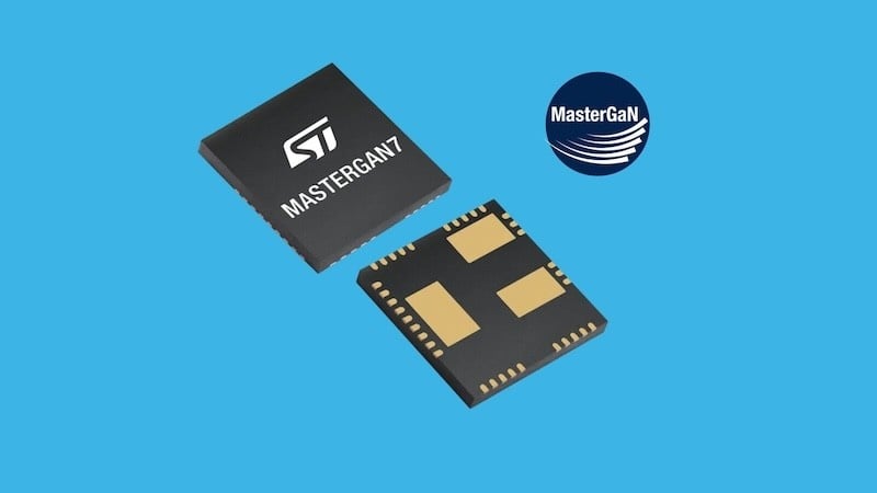
STMicro’s MasterGaN7 transistor
By co-packaging the power switches with matched driving circuitry in a unified surface-mount form factor, the MasterGaN7 eliminates parasitic gate-loop inductances, streamlines board layout, and minimizes overall system component count.
Integrated GaN Half-Bridge Architecture
The core of the MasterGaN7 comprises two 650 V GaN power transistors configured as a half-bridge with typical on-resistance () of 270 mΩ and a continuous drain-current rating of up to 6 A at 25°C. Because GaN transistors do not possess an intrinsic p-n junction body diode, the MasterGaN7 exhibits zero reverse-recovery charge (). This eliminates reverse-recovery losses during commutation, enabling hard-switching and soft-switching topologies to operate at peak efficiency.
The device integrates low-dropout (LDO) linear regulators on both the low-side and high-side driver rails, providing a stable 6 V supply directly to the internal gate driver output stages. This tightly controlled gate-drive voltage ensures consistent turn-on dynamics across operating temperatures without requiring discrete external voltage regulators.
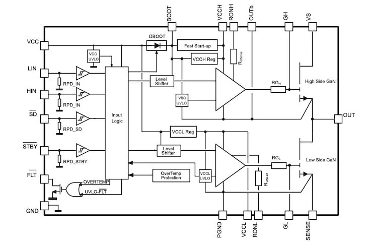
Block diagram of the MasterGaN7
The high-side floating driver section is biased via an integrated bootstrap diode structure connected between the VCC and BOOT pins, simplifying floating rail generation and further shrinking the external bill of materials (BOM). More information can be found in the MasterGaN7 data sheet.
High-Frequency Dynamics and Control Interface
Operating with a driver propagation delay of 45 ns and capable of handling input pulse widths down to 35 ns, the MasterGaN7 supports switching frequencies up to 2 MHz. The fast switching speeds allow engineers to scale down the physical footprint of magnetic cores and passive filter capacitors:
- Slew Rate Control: Dedicated low-side () and high-side () pins allow developers to adjust turn-on gate resistors with external discrete resistors (0 Ω to 220 Ω), tailoring switching slew rates (up to 120 V/ns) to optimize electromagnetic interference (EMI) performance.
- Logic Compatibility: The input logic stage accepts 3.3 V to 15 V typical levels (and up to 20 V maximum) with built-in Schmitt triggers and internal pull-down resistors, facilitating direct interfacing with standard microcontrollers, DSPs, or analog PWM controllers.
- Standby and Low-Power Operation: An active-low standby pin () places the device into a low-quiescent-current state, drawing approximately 500 µA, to maximize no-load and light-load burst-mode efficiency. A dedicated shutdown pin () provides immediate disabling of the switching stages within 70 ns.
Hardware Protections and Thermal Design
To safeguard power architectures under abnormal conditions, the MasterGaN7 incorporates multiple protection mechanisms directly on silicon:
- Cross-Conduction Prevention: Hardware interlocking logic prevents both GaN transistors from conducting simultaneously, even if conflicting control pulses appear at the inputs.
- Undervoltage Lockout (UVLO): Independent UVLO circuits monitor the VCC rail, low-side driver stage, and high-side floating bootstrap rail, keeping the power switches safely off during power-up or bus sag.
- Thermal Shutdown: Built-in overtemperature protection trips at 175°C with a 20°C hysteresis, automatically placing the power stage into a high-impedance state during thermal runaway.
- Fault Signaling: An open-drain active-low fault pin () pulls low when UVLO, standby mode, or thermal faults occur, allowing real-time telemetry back to the system processor.
The module is housed in a low-profile 9 mm × 9 mm × 1 mm QFN package featuring three separate exposed thermal pads (GND, SENSE, and OUT) to route heat efficiently into internal PCB copper planes, achieving a low junction-to-case thermal resistance () of 2.8°C/W. The package maintains standardized creepage distances between high-voltage and low-voltage pin groupings to adhere to industrial isolation requirements.
Target Topologies and EVLMG7 Evaluation Support
The MasterGaN7 is suited for mid-power AC-DC and DC-DC conversion across industrial and consumer sectors. Primary topologies include active-clamp flyback (ACF), asymmetrical half-bridge (AHB), high-voltage resonant LLC converters, buck and boost converters, and high-voltage totem-pole power factor correction (PFC) stages. Target end-equipment includes:
- High-density USB-PD fast chargers and laptop power adapters.
- Solar microinverters and residential energy storage systems.
- Industrial LED lighting drivers and switch-mode power supplies (SMPS).
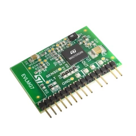
The EVLMG7 is a GaN-based half-bridge power module equipped with MASTERGAN7. It can quickly create new topologies without needing a complete PCB design.
To shorten development timelines, ST provides the EVLMG7 evaluation board. Designed as a 30 mm × 40 mm plug-and-play daughterboard, the EVLMG7 allows power designers to drop the MasterGaN7 directly into motherboard prototypes—such as resonant LLC and PFC platforms—without requiring an immediate custom high-voltage layout. The board provides access to all control signals, on-board bootstrap networks, and adjustable low-side shunt resistor footprints for peak-current mode control.
Availability and Pricing
The MasterGaN7 is in volume production and available now in tape-and-reel packaging (order code: MASTERGAN7TR). Pricing begins at $3.83 each in quantities of 1,000 units. The companion EVLMG7 evaluation board is available through the STMicroelectronics eStore and authorized global distributors.
All images used courtesy of STMicroelectronics.
Related Content