Facebook
 Google
 GitHub
 Linkedin
SimpleChips Technology Unveils its Space-Saving 1200V, 15A High-Side Switch
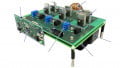
The new unit is complete in a single TO-263 package, replacing the multiple discrete components otherwise required
In current practice, engineers implement high-side switches by combining a MOSFET or IGBT with the necessary gate drivers and the additional components needed to tie them all together. SimpleChips’ new 16SCT100 eliminates the necessary design process and also frees up the board space that the result would require.

The 16SCT100 saves design time and frees up board space. Image used courtesy of SimpleChips
Enabling More Compact OEM designs
As described by Alain Comeau, CEO and CTO at SimpleChips Technology, “Over the past years, we have developed very small high voltage Gate Drivers for medical implant devices, and by reusing our technology we developed a product we believe will enable more compact products”
The new unit provides sufficient creepage distances to obviate the need for PCD slots or conformal coating. Another key feature of the 16SCT100 is its excellent power efficiency, made possible through its very low on-resistance of 210 mΩ and its low high-voltage off current of 260 µA.
Functional Description
The unit operates at frequencies of 10 kHz and below. Energy losses are low, at 140uW/A. The 16SCT100 is most suited to drive resistive loads, but inductive loads can also be handled if appropriate cautions are observed.
Definitions for the Functional Block Diagram
- Vss: Pin #1, Ground
- Vdd: Pin#2, Low voltage supply
- Input: Pin #3, Input signal (CMOS level logic)
- Source: Pin #4, Output FET Source
- HV: Pin #5, High voltage supply

Functional block diagram of the 16SCT100. Image courtesy of 16SCT100 datasheet.
Absolute Maximums
- HV power supply (HV - Vss) and HV to source voltage (HV - Vs) are both 1200 V
- Maximum negative source voltage is -500 V
- Source currents, continuous and pulsed (@25C) are 15 and 19 amps, respectively
- Vdd power supply (Vdd - Vss) is 18V
- Junction temperature. The 16SCT100 operates over a junction temperature range of -40 to +150℃
Recommended Operating Voltage Minimums and Maximums
The first figure is the minimum, the second figure is maximum
- HV – Vss: 40 and 1000 volts
- HV – Source: 0 and 1000 volts
- Vdd – Vss: 6 and 18 volts
Application Notes
The new unit is a high-side switch often used to implement H-Switches, which are employed to switch the polarity of the voltage applied to a load. For the interested reader, we detail
H-bridges in a previous article.

H-Bridge. Image courtesy of 16SCT100 datasheet
In dealing with inductive loads, users of the 16SCT100 need to observe some cautions concerning the allowable negative transient source voltage, which is a function of HV.
The details are described in the datasheet. When driving inductive loads in discontinuous mode, the circuits must deal with “ringing” that follows the cutoff to the load. As an example, with HV at 400 volts, the device can tolerate negative transients of as much as 300 volts, but no more.
Within this range, there will be no need for engineers to include anti-parallel diodes in their circuit designs.
About SimpleChips
SimpleChips Technology Inc. is a global provider of analog and mixed-signal integrated circuits for medical, industrial, and military applications.