Facebook
 Google
 GitHub
 Linkedin
Onsemi Unveils Interactive Web Tool to Simplify Power Design
The new Elite Pairing Studio is an interactive cloud-based simulation tool designed to give power electronics engineers deep visibility into device-level switching behavior and component trade-offs.
Today, ahead of PCIM, Onsemi has introduced its new Elite Pairing Studio, an online design tool tailored to simplify the pairing of silicon carbide (SiC) MOSFETs and gate drivers. Focused on demanding power electronics applications—such as AI data centers, electric vehicles, and industrial systems—the tool moves beyond traditional component-level selection to give engineers early visibility into device-level behavior and trade-offs.

Onsemi’s Elite Pairing Studio is an online design tool tailored to simplify the pairing of silicon carbide (SiC) MOSFETs and gate drivers.
Power electronics architectures are growing more complex and, as a result, properly matching gate drivers with switching devices is critical to achieving optimal efficiency, minimizing losses, and ensuring safe operating temperatures. This process tends to require time-consuming manual evaluation, extensive datasheet comparisons, spreadsheet analysis, and empirical testing.
The Elite Pairing Studio simplifies this engineering challenge by guiding users through an intuitive workflow to quickly identify well-matched component combinations based on specific system requirements.
Automated Workflow and Data-Driven Selection
The cloud-based environment provides a private, secure workspace on Onsemi.com where engineers can analyze a wide range of gate driver combinations alongside a selected SiC MOSFET. The platform automatically evaluates options using transparent evaluation logic grounded in established industry equations and real-world performance calculations.
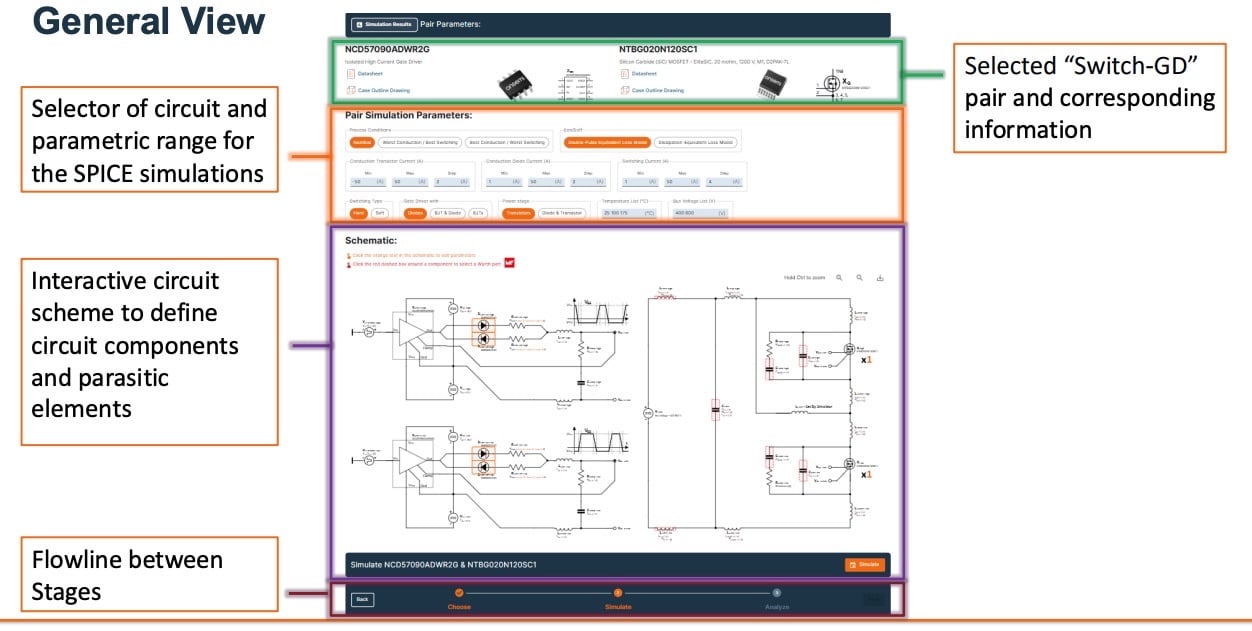
During the simulation step, the Elite Pairing Studio generates detailed switching waveforms for the selected MOSFET and gate‑driver combination using onsemi’s physics‑based SPICE models. (Click on image to enlarge).
Rather than manually cross-referencing disparate documentation, designers can leverage clear, inspectable logic to evaluate well-matched pairings. This upfront optimization allows engineering teams to refine power architectures and make better-informed decisions early in the development cycle, significantly reducing design risk, shortening time to market, and lowering downstream iterations.
Physics-Based Simulation and Waveform Analysis
A core benefit of the Elite Pairing Studio is its ability to generate interactive, personalized simulations under realistic operating conditions. The environment provides engineers with deep visibility into timing, waveform behavior, and the precise trade-offs behind each recommended pairing.
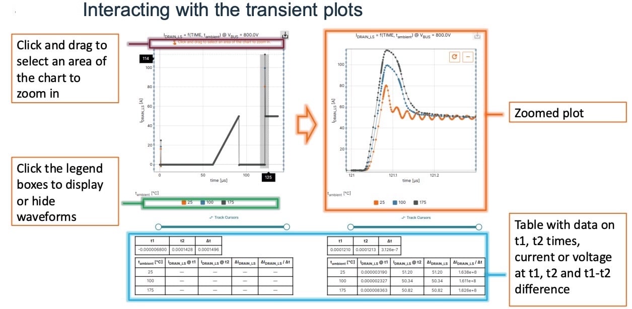
Elite Pairing Studio consolidates the simulation results to provide a clear comparison of how each gate driver performs with the selected SiC MOSFET. (Click on image to enlarge).
Through an integrated interactive waveform viewer, designers can inspect crucial figures of merit for each evaluated pairing. These include:
- Switching Timings: Engineers gain clear insight into precise timing parameters during device activation and deactivation.
- Waveform Behavior: The viewer displays detailed gate voltage and current (V/I) waveforms to evaluate transient states.
- Voltage Overshoot Margins: Users can inspect voltage overshoot margins relative to maximum device ratings to verify safety and reliability margins.
- Switching Energy Losses: The tool calculates specific turn-on and turn-off energy losses to optimize efficiency.
These data-driven insights give engineers early visibility into factors influencing electromagnetic interference (EMI) behavior and reliability margins before advancing designs to full system-level analysis.
Seamless Integration into System-Level Analysis
The Elite Pairing Studio acts as the "front door" to Onsemi's broader suite of simulation and design tools. Once an optimal device pairing is established, the studio generates PLECS system-level simulation models.
These pairing insights can be carried forward directly into the Onsemi Elite Power Simulator to fine-tune system-level efficiency, thermal behavior, and loss performance. This seamless development path streamlines the translation of early-stage component selection into improved system efficiency for next-generation electrification infrastructure, industrial systems, and AI data centers.
Availability and Future Outlook
The Elite Pairing Studio is available now through the Onsemi website. The company will also demonstrate the interactive design platform at the Onsemi booth (Hall 9-332) this week during the PCIM Expo 2026 in Nuremberg, Germany. While the initial launch focuses on SiC MOSFETs and gate drivers, Onsemi plans to expand the studio's capabilities by adding additional technologies in the future.
All images used courtesy of Onsemi.