Facebook
 Google
 GitHub
 Linkedin
Nexperia’s 650V GaN FETs Sport RDS(ON)s of 33 Milliohms
The new devices will enable power supplies functioning at 2 kW and higher to satisfy the 80 PLUS Titanium standard
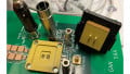
Nexperia’s second-generation 650 volt H2 power GaN FET device family targets single phase AC/DC and DC/DC industrial switched mode power supplies (SMPS), ranging from 2 kW to 10 kW.
s_of_33_Milliohms_Fig1.jpg)
Image courtesy of Nexperia
The 650V H2 power GaN FETs feature a 36% shrinkage in die size when compared to devices specced at similar RDS(ON) values. The units are packaged with a second semiconductor, a low-voltage silicon MOSFET device in the now-classic cascode configuration. The job of the second device is to trigger the H2 GaN HEMT itself, eliminating the need for separate driver circuitry.
s_of_33_Milliohms_Fig2.JPG)
The H2 power GaN FET internal diagram. Image courtesy of Nexperia
By eliminating the need for complicated drivers, costs, BOM and time to market are all decreased.
What is The Titanium Standard?
CLEAResult describes the 80 Plus Standard in detail. As explained by Dilder Chowdhury, Nexperia’s GaN Strategic Marketing Director, “Titanium is the most demanding of the 80 PLUS specifications, requiring >91 % efficiency under full load conditions (>96% at 50% load). Achieving this level of performance in server power applications operating at 2 kW and above, using conventional silicon components, is complex and challenging. Nexperia’s new power GaN FETs are ideally suited to an elegant, bridgeless totem pole configuration that uses fewer components and reduces both physical size and costs.”
The Newest Members of the Family
The newest members of the family include:
- The GAN039-650NTBA
- The GAN039-650NBBA
- The GAN039-650NTB
- The GAN039-650NBB
Clicking on any of the four above devices leads to its datasheet. However, these devices are still largely in development, so many specifications are not yet available
All four devices feature maximum drain source voltages of 650 volts, maximum drain current of 60 amps, and total power dissipations of 300 watts. The units are all n-channel, normally on devices.
Common Characteristics
- Gate drain charge (QGD) 5 nC
- Total gate charge (QG) 30 nC
- Recovered charge (QR) 150 nC
- Maximum gate-source voltage is fron -20 to +20 volts
- Typical gate-source threshold voltage is 4 volts
- Maximum thermal resistance from junction to mounting base is 0.5 °K/watt
Differences
- The GAN039-650NTB and the GAN039-650NTBA are available in surface mounted copper clip inverted package (CCPAK1212i)
- The GAN039-650NBB and the GAN039-650NBB come in non-inverted surface mounted copper clip packages (CCPAK1212)
- The GAN039-650NTBA and the GAN039-650NBBA are aimed at automotive use
Applications
- Automotive on-board-chargers
- Hard and soft switching converters
- Severs and other telecom applications are required to meet 80 PLUS Titanium standards
- Solar and UPS inverters
- Bridgeless totem pole power factor correction (PFC)
- Servo motor drives
- Electric vehicle (EV) drivers and controllers
- Power supplies for 5G
Physical Considerations
- The units are available in CCPAK1212 packages. Both CCPAK1212 and CCPAK1212i versions feature maximum dimensions of 12.3 mm (including gull wings) x 11.1 mm
- Amenable to automated optical inspection (AOI)
- Operate over a junction temperature range of -55 to 175℃
Regulatory Considerations
The GAN039-650NTBA and the GAN039-650NBBA are qualified to AEC-Q101