Facebook
 Google
 GitHub
 Linkedin
NEC Electronics America Broadens Lineup Of Low-Power 32-Bit All Flash Microcontrollers For Portable Devices
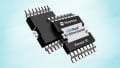
NEC Electronics America, Inc. expanded its lineup of low-power 32-bit V850ES/Jx3™ All Flash™ microcontrollers (MCUs) with the new V850ES/Jx3-L™ MCUs, which are said to offer the lowest standby current in their class to help meet stringent power requirements in battery-backed multiphase electricity meters, high-end blood glucose meters, test and instrumentation equipment, point-of-sale systems and other high-end portable devices that demand high performance, low power consumption and an extensive variety of integrated peripherals.
Backward compatibility with earlier generations of NEC Electronics’ V850™ All Flash MCUs are said to provide designers with an easy upgrade path, while compatibility with other MCUs in the V850ES/Jx3 lineup is said to give designers the flexibility to select from a variety of compatible devices with higher performance and up to one megabyte (MB) of on-chip memory. Due to improvements made by NEC Electronics, the new devices consume only 0.9mW of power per Dhrystone MIPS (DMIPS) during active operation, and as little as 1.5µA in standby mode.
In addition to NEC Electronics’ V850ES™ RISC CPU core and a pipeline architecture that executes up to 43 DMIPS (1.1) at clock speeds ranging from 5 to 20 MHz, the V850ES/Jx3-L MCUs offer flash memory capacities of 128 or 256 KB, embedded RAM up to 16 KB, operating voltages from 2.2 to 3.6V and an I/O tolerance of 5V. The new MCUs also feature enhanced, integrated digital signal processing (DSP) capability, including divide/multiply functions for high-end applications such as motor control and metering.
To further reduce component count and system cost, the MCUs include up to three UART channels, three I²C channels or five clock serial interface (CSI) channels, a built-in cyclic redundancy check (CRC) circuit, an advanced hardware multiplier for fast execution of algorithms and an external bus interface that supports expanded memory. One channel of 16-bit watchdog timer with a dedicated internal oscillator, a watch timer, up to 12 channels of 10-bit A/D conversion, up to two channels of 8-bit D/A conversion, a direct memory access (DMA) controller with four independent DMA channels, a two-level low-voltage detector, a real-time output port and an on-chip debugging circuit with interrupt functionality complete the MCUs’ highly integrated design.
The MCUs are available in 80- and 100-pin low-profile quad flat pack (LQFP) packages. The 80-pin LQFP is available in standard 14 x 14 or 12 x 12mm sizes that further contribute to miniaturization in portable equipment. The 100-pin LQFP is available in fine-pitch 14 x 14 or 14 x 20mm versions.
Pricing varies according to memory configurations. For example, the 100-pin V850ES/JG3-L MCU with 256KB of flash memory and 16KB RAM is $6.00 each in sample quantities. Dedicated starter kits are expected to be available in summer 2008. Mass production of the 100-pin version is scheduled for the end of July 2008.