Facebook
 Google
 GitHub
 Linkedin
IXYS Introduces New Rugged 500 and 600V PolarP3 Power MOSFETs
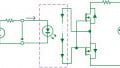
IXYS Corp. announced the release of its new PolarP3™ Power MOSFET family. The company says the announcement represents a signification addition to its extensive high-performance Polar-Series Power MOSFET product line. These new devices combine IXYS’ latest Polar-Series technology platform and HiPerFET™ process to deliver a Power MOSFET solution that exhibits benchmark electrical and thermal characteristics. These characteristics include low on-state resistances (Rdson as low as 39mΩ), low gate charge (Qg as low as 33nC), low thermal resistances (Max Rthjc as low as .066°C per watt), high power dissipation (Pd as high as 1890W), superior dV/dt performance and high avalanche energy capabilities. These outstanding electrical and thermal device attributes allow for improved power efficient topologies in applications such as power factor correction circuits, switch-mode powers supplies, UPS, motor drives, lamp ballasts, laser drivers, dc-dc converters, battery chargers, solar generation systems, robotic and servo control.
The new Power MOSFETs are initially available in two voltage grades: 500V and 600V grade respectively. 500V PolarP3 offerings include drain current (Tc = 25°C) ratings of 60, 78, 98, 112 and 132A. Conversely, 600V PolarP3 offerings will include drain current (Tc = 25°C) ratings of 22, 28, 42, 50, 64, 80, 90 and 110A. These new devices feature a very desirable low FOM (Figure of Merit: Rdson x Qg) performance index as low as 9.6Ω-nC, providing substantial reductions in both the conduction and switching losses of the device, thereby enabling increased efficiency and reduced power consumption in power conversion systems.
High speed switching applications such as switch-mode power supplies (SMPS) and uninterruptible power supplies (UPS) will greatly benefit from the ultra-low total gate charge and gate drain charge (Qg=38nC, Qgd=11nC, Vgs at 10V) characteristics of these devices. The low gate charge and gate drain charge characteristic allows designers the ability to boost power conversion efficiency through the use of high-speed switching and to promote the use of smaller passive components, thus freeing up additional PCB real estate and reducing the cost of bulky passive components. In additional, the low gate charge reduces the amount of gate drive power requirement (Gate Drive Power = Qg x Vgs x Fsw) for the Power MOSFET to fully conduct. Since these devices require less gate drive power, simple economical gate drive solutions can be implemented, further reducing cost and complexity.
Power switching capabilities and device ruggedness of these devices is further enhanced through the utilization of IXYS’ HiPerFETTM process, yielding a device with a fast intrinsic diode for low reverse recovery charge (Qrr) and improved turn-off dV/dt immunity. The enhanced dV/dt capability of these devices offers significant safety margins for the stresses encountered in high-voltage switching applications. Furthermore, these new devices eliminate the need for discrete anti-parallel high voltage diodes used in conventional designs, thereby reducing part count, simplifying PCB layouts, reducing overall losses and improving power density. The featured fast intrinsic body diode properties of these HiPerFETs play a pivotal role in overall device performance by providing faster transient response, increased power efficiency, improved ruggedness, and higher operating frequencies and making them ideal for use in critical high switching applications such as switch-mode power supplies.
Initial package housing availability of these new devices is available in various industry standard packages. These packages include the TO-247, TO-3P, TO-268, TO-264, SOT-227, PLUS264, and PLUS247.