Facebook
 Google
 GitHub
 Linkedin
High-Voltage Devices Improve Power Density and Conversion Efficiency
High-voltage devices from Power Integrations and Magnachip Semiconductor use the latest gallium nitride and silicon power technologies and advanced packaging to raise the bar for power density and conversion efficiency.
High-voltage field effect transistor (FET) devices are essential to power conversion systems as industrial and other applications migrate to higher voltage levels for greater efficiency. Two devices are innovating advances in materials and packaging to optimize the functions of FETs.

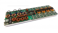
Servers powered with high-voltage GaN devices. Image used courtesy of Power Integrations
Power Integrations has released a single-switch gallium nitride (GaN) power supply chip built with a 1250 V device using the company’s PowiGaN technology. The InnoSwitch3-EP 1250 V is the latest of Power Integrations’ InnoSwitch series of single-switch, flyback power ICs rated from 725 V to 1700 V and constructed with silicon, silicon carbide (SiC), and PowiGaN gallium nitride (GaN) power switch technologies.
Magnachip Semiconductor has introduced three silicon-based Super Junction Metal Oxide Semiconductor Field Effect Transistors (SJ-MOSFET).
Using the latest microfabrication technology, a 600 V SJ-MOSFET device in a Decawatt Package (DPAK) narrows cell pitches by 50%, resulting in a 42% reduction in on-resistance (RDS(ON)).
Magnachip’s two 650 V SJ-MOSFET power switches feature a PDFN88 package that reduces device height by up to 81% compared to similar D2PAK packaged devices.
InnoSwitch3-EP Power Management ICs
Power Integrations’ family of InnoSwitch3-EP power management ICs are multi-mode, quasi-resonant, CCM flyback controllers that integrate a power switch and provide secondary-side sensing and synchronous rectification drive control.
Each model in the InnoSwitch3-EP family uses the same design but incorporates different power switch technologies. The InnoSwitch3-EP 1250 V device features an internal 1250 V GaN device and will join prior models with integrated 750V/900 V silicon MOSFET, 750V/900 V gallium nitride PowiGaN and 1700 V SiC Switch devices.

InnoSwitch3-EP single-switch flyback topology. Image used courtesy of Power Integrations
According to Radu Barsan, Vice President of Technology at Power Integrations, the 1250 V GaN variant of the InnoSwitch3-EP series will extend the application space for GaN power devices, including those currently served by silicon carbide.

InnoSwitch3-EP power switch technologies. Image used courtesy of Power Integrations
With a 1250 V rating, the InnoSwitch3-EP 1250 V can be specified for operating voltages up to 1000 V with an adequate margin for voltage limitations and is ideal for industrial and power grid applications that demand robustness.
Smaller, More Efficient Power MOSFETs
The MMD60R175S6ZRH is a 600 V SJ-MOSFET from Magnachip constructed on a 180 nm process node. According to Magnachip, the microfabrication process technology narrows cell pitches for the device by up to 50%. The result is an on-resistance (RDS(ON)) that is about 40% lower than prior devices (175 mΩ) with the same DPAK form factor.
The devices have a gate charge nearly 30% lower than prior generations, resulting in fewer switching losses and better power conversion efficiency.
The MMD60R175S6ZRH suits various applications, including servers, OLED TVs, and laptop fast chargers.

6th generation 600V SJ MOSFET. Image used courtesy of Magnachip
Magnachip is also expanding its low-profile SJ-MOSFET portfolio by introducing two 650 V devices in a thin PDFN88 package. With the new packaging, the MMUB65R090RURH and MMUB65R115RURH boast a height profile over 60% less than similar DPAK packaged devices that typically have heights above 2 mm.
In applications like OLED TVs, component heights can significantly affect display size, quality, and cost. The new devices are also efficient with on-resistances down to 90 mΩ.
Related Content