Facebook
 Google
 GitHub
 Linkedin
How GaN Devices in TOLL Packaging Improve Efficiency in Solar Applications
GaN devices in TOLL packages boost solar inverter efficiency and compactness. Learn how this technology provides great thermal performance, low parasitics, and multi-source compatibility.
With ever-growing demand for renewable energy, there is a need for efficient, compact and cost-sensitive power-conversion systems. For example, a photovoltaic panel generates a DC voltage that has to be converted to an AC grid voltage with an inverter. Inverter efficiency directly impacts solar panel efficiency (Figure 1), which in turn impacts the overall return on investment.
Another example in residential solar installments is the need to optimize roof space to fit as many panels and inverters as possible, which requires compact, cost-effective inverters.

Figure 1. GaN devices in TOLL packages offer a way to improve power conversion efficiency in solar inverters.
To address these challenges, consider using gallium nitride (GaN) devices for power converters in the transistor outline leadless (TOLL) package. A TOLL package has a large thermal pad at the bottom that helps with efficient heat dissipation, enabling the use of a relatively cheaper heat sink to save costs. GaN devices have an integrated driver thus simplifying the layout and saving area on the printed circuit board (PCB).
TI GaN devices in the TOLL package also have features such as zero voltage detection, zero current detection and a low-dropout 5 V output, while being pin-to-pin compatible with discrete GaN devices in a TOLL package, thus being multisource compatible
Introduction to TOLL Packaging
A TOLL package is a surface-mount package designed for high current applications in automotive and industrial applications. It offers better thermal dissipation and lower parasitics compared to surface-mount packages such as the double decawatt package (D2PAK) or transistor outline (TO)-247 package.
Being a leadless package, the TOLL package’s parasitic inductance is very low, which results in faster switching (reducing switching losses) while also helping lower electromagnetic interference. The dimensions of a TOLL package are 9.9 mm by 11.68 mm by 2.3 mm, which is significantly smaller than the TO-247, at 15.94 mm by 20.95 mm by 5.02 mm, and would result in 70% higher area on PCB. An optimized GaN process enables GaN field effect transistors (FETs) with very low RDS (on), suitable for high-power applications.
Comparisons to IGBTs and SiC
GaN is rapidly replacing insulated-gate bipolar transistors (IGBTs) and silicon carbide (SiC) devices in power converters given advantages such as better resistance per die area (Rsp), lower input and output capacitances, and zero reverse-recovery charge. GaN in TOLL packaging further improves performance.
GaN has a better RDS (on) Rsp, which helps lower conduction losses while maintaining switching losses, as the output capacitance per die size is lower. GaN can switch at a higher frequency compared to silicon and SiC solutions that helps reduce the size of magnetics, making overall systems compact and light. TOLL packaging has a lower lead inductance that supports higher slew rates.
Energy Infrastructure Applications
Solar microinverters, string inverters, power optimizers and energy storage systems each have power-conversion stages that can use GaN to improve efficiency, which can lead to more compact and cost-effective products.
In the case of a power optimizer or a maximum power point tracking (MPPT) in a string inverter, supporting the maximum power point tracking of higher-power panels (which can reach wattages as high as 1,000 W per panel), switching devices with balanced conduction and switching losses are necessary as these systems don’t have a heat sink due to space constraints. TOLL GaN is the right solution here to maintain the temperature rise of the system.
Design Tips for GaN Devices in TOLL Packaging
GaN devices in the TOLL package have an integrated gate driver to drive the GaN FET while having the same pinout as discrete TOLL devices. In this section, I’d like to address some design and layout tips to help you choose the right device and lay it out on the board.
The Trade-Off Between RDS (on) and Coss
Your first big decision is to choose the right RDS (on) for your application because it directly affects conduction losses in the system. A lower RDS (on) requires a larger GaN die which increases the output capacitance (Coss) and in turn the switching losses. Larger dies are also expensive.
If you are using a hard-switching topology, then you will likely have to consider a trade-off between conduction and switching losses after calculating them. Very low RDS (on) is not preferable here, as the switching losses will be higher than the conduction losses.
On the other hand, for a soft-switching topology, a lower RDS (on) would improve efficiency, with negligible switching losses. If the topology is hard-switched at lighter loads, then lighter loads will have higher losses. Decide based on your design requirements.
Codesigning with TI and Discrete GaN Devices in TOLL Packaging
TI GaN devices in the TOLL package have an integrated gate driver to drive the GaN FET, whereas discrete GaN devices in TOLL packaging from competitors use an external gate driver. Designers always look for multisource compatibility in their designs. With only minimal changes, it is possible to use the TI device and discrete device in the same PCB.
As shown in Figure 2, you can use the same schematic with some modifications to accommodate both TI and discrete GaN devices on the same PCB.
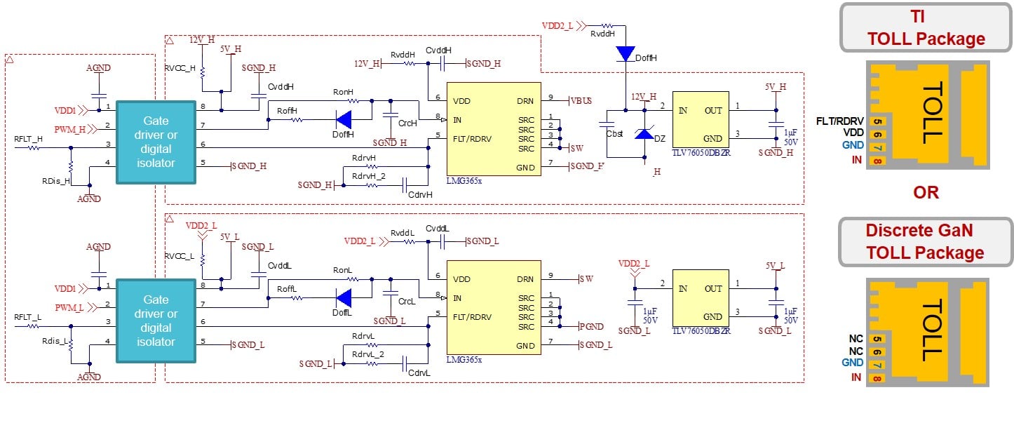
Figure 2. Common schematic for TI and Discrete TOLL GaN. (Click on image to enlarge)
Addressing Key Challenges
GaN devices in TOLL packaging address key challenges in power conversion, offering improved thermal performance, higher efficiency, and compact form factors. These advantages make them well-suited for applications in energy infrastructure, solar inverters, and industrial systems where space, performance, and reliability are critical.
As GaN FET technology continues to mature, it is enabling system designers to meet increasing power demands without compromising on size or efficiency. By simplifying layout and enhancing thermal management, TOLL-packaged GaN devices contribute to more robust and scalable designs—ultimately helping engineers deliver more efficient, compact, and cost-effective solutions across a wide range of power applications.
All images used courtesy of Texas Instruments.
Related Content