Facebook
 Google
 GitHub
 Linkedin
Future-Proof Power Module Package for High-Power Applications
While the XHP 2 power module package from Infineon Technologies AG is designed for use in today’s applications, it also meets the requirements of future-oriented applications. The package supports the outstanding performance of the 1.7 kV IGBT5 with its. XT joining technology, which is suitable for a continuous operating temperature of 175°C and for the demanding module characteristics of future generations of SiC MOSFETs.
Different applications require different module requirements. In line with this, Infineon’s XHP 2 module package addresses voltage classes from 1.7 kV to 3.3 kV for different platforms [1]. For some applications, however, there are certain design challenges that need to be addressed. These include the large creepage distances for high-voltage classes and the closely spaced DC terminals for fast-switching SiC MOSFETs required to obtain a symmetrical and low-parasitic commutation inductance.
Multiple Requirements Shaped the XHP 2 Design
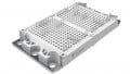
In figure 1a, the arrangement of the DC(+) and DC(-) terminals are depicted. The DC terminals are arranged in two rows to build a stripline bus bar with a resulting low module inductance of Ls<10 nH. This low module inductance enables a very low inductive commutation loop for the design of the application. Without compromising this design, the terminal has been designed to provide the required creepage distance for the 3.3 kV voltage class. With respect to clean switching behavior [2], the switching technologies in all voltage classes will benefit from the low-inductive design, and also simplify the hardware designer’s job.
For the control board, the auxiliary connections are spaced at a suitable distance from the sides at the center of the module to allow the proper creepage distances on the printed circuit board (PCB). Furthermore, if the modules are connected in parallel per phase and mounted side by side, the aux terminals for the top and bottom system are aligned in the corresponding rows so that equivalent control terminals can be simplified and connected from one module to the next.
As depicted in figure 1b, the height of the control terminals enables a double-sided PCB to be mounted on top of the module, offering an additional degree of freedom for the PCB designer.

a)

b)
Figure 1. a) Typical appearance of XHP 2; b) Aux terminal height. Image used courtesy of Bodo’s Power Systems
Thermal Aspects of Module’s Main Terminals
For power modules with the IGBT5/.XT generation of silicon (Si) chips, the targeted current capability is at least Inom=1800 A. In conjunction with the high current capability, the package has to be able to withstand the established operation temperature of this IGBT5/.XT, which is Tvj,max=175 °C. This temperature target should also be considered for extreme situations with low-voltage applications, when the package must transfer high currents, such as in low-voltage ride-through (LVRT) grid faults of a wind turbine at the same time. Due to these challenges, the temperature and the current capability of the terminals are key.
As the ohmic loss is proportional to the square of the current, heat dissipation is an important issue for both the module and the laminated DC busbar in the application assembly. The design of Infineon’s XHP 2 power terminal respects this application-relevant interface. In addition to the DC terminals, the RMS current in the AC terminals also needs to be considered. Which, in relation to the DC current, is higher by a factor of √2. Because of this relation, three single AC terminals combined with a superior thickness for high-current capability are provided.
With an expectation of increasing phase-leg current with new chip generations, the Pout, terminal behaves disproportionately. Thus, for higher output current densities, it is essential to dissipate terminal-generated losses to the environment at the system level.
DC Terminal IR Measurements
Besides the simulations carried out in the development phase when creating the mechanical design, the terminal temperature under load was measured and verified by infrared (IR) tests on the hardware. The DC connections, which are typically contacted with sealed laminated busbars, offer few opportunities to dissipate the power loss by natural convection. For this investigation, an open, black-coated XHP 2 module, with a mounted DC-link busbar on the DC terminals, was tested under high continuous load conditions.

Figure 2. Infrared measurement and temperature of an open, black-coated module; DC terminals under DC-load condition IDC=876 A show a temperature at screw position of Tterminal,DC(+/-)~110°C. Image used courtesy of Bodo’s Power Systems
Figure 2 depicts the infrared test results of the DC terminals. A high DC current of IDC=876 A, ~50 percent of Inom is equivalent to a phase-leg current of around Iphase,leg=1238 A. The current flows from the DC(-) terminal to the low side diode then to the high side diode and back through the DC(+) terminal. This current is heating up all diodes in the module to 175°C. The module is mounted on a liquid-cooling plate, and the resulting case temperature is measured at TC~120 °C. The temperature under such harsh conditions in the connection area (at the screws) between the module DC terminal and the DC busbar is below 125°C. Based on these results, no critical values could be detected on the DC terminals of the power module, which confirms the high-current and high-temperature capability of Infineon’s XHP 2 design.
Dynamic Switching Characteristics
The module circuit for a single module is made in a half-bridge configuration. In figure 3, the circuit diagram and the top view of the module with electrical connections are depicted. Besides the required gate-emitter control terminals, additional aux-mainemitters, connectors 8 and 12 marked in red are provided. These additional terminals enable the option for the usage of the voltage drop of the leakage inductance, if a more sophisticated gate-control design is required [3].
Figure 4 illustrates the IGBT turn-on, turn-off and diode recovery at Tvj=175°C and 25 °C of an FF1800XTR17T2P5 power module with IGBT5/.XT under the nominal conditions of UDC=900 V, IC nom=1800 A from a double-pulse test.

Figure 3. Circuit diagram of the XHP 2 power module. Image used courtesy of Bodo’s Power Systems
In figure 4a, examples from the turn-off tests show, with a total stray inductance of LS~30 nH for the setup, the overvoltage shoot at ΔUCE~300 V is low, which demonstrates another advantage of the low-inductive mechanical design. All other switching events shown in the turn-on in figure 4b, and the diode commutation behavior in figure 4c show smooth waveforms and characteristics without snap-off or oscillation effects.
The mechanical design of the power terminals DC(+) and DC(-), as shown in figure 1, is optimized for the paralleling of modules. As shown in the example in figure 5, the IGBT turn-on switching behavior of two hard, parallel-connected modules is presented. The current sharing of the devices is very similar. There is no current mismatch affected by the DC busbar design described in [4], [5].

(a)

(a)

(b)

(b)

(c)

(c)
Figure 4. IGBT a) turn-on, b) turn-off and c) diode recovery at nominal conditions of an FF1800XTR17T2P5 at Tvj=175°C and 25°C power module. Image used courtesy of Bodo’s Power Systems
Summary of Application-oriented Module Design
Infineon’s XHP 2 power module design strictly adheres to the requirements of a low-inductance and symmetrical design and has served as a template for this housing class. The module equipped with the 1.7 kV IGBT5/.XT will be serving light rail applications, on and off-shore wind turbine applications, and any other demanding application where reliability and robustness are system relevant.

Figure 5. IGBT turn-on of two modules in parallel. Blue represents the left module and red the right module. Image used courtesy of Bodo’s Power Systems
According to the principle “form follows function,” the creepage distances of the housing correspond to the 3.3 kV voltage classes. These distances have been implemented without compromising the low-inductance and symmetrical design, which enables the use of advanced SiC MOSFET components on the same platform.
The power loss of the terminal is a key application-design issue and the design of the module has thus optimized terminal losses accordingly.
Based on these features, the Infineon XHP 2 can indeed be called an application-oriented, multi-package housing designed for the next generation of high-power applications.
This article originally appeared in Bodo’s Power Systems magazine.