Facebook
 Google
 GitHub
 Linkedin
Fairchild MicroFET MOSFET Shrinks Its Footprint for Portable Designs
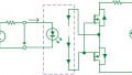
Fairchild Semiconductor introduced a portfolio of MicroFET™ MOSFETs packaged in an ultra-compact and thin footprint (1.6 x 1.6 x 0.55mm). The company states that designers can select the MicroFET MOSFET that optimally suites their application and design needs. This new portfolio contains a number of commonly used topology choices, including, single P-Channel and Schottky diode combo, single N-Channel and Schottky diode combo, dual P-Channel, dual N-Channel, complementary pair, single N-Channel and single P-Channel.
These MicroFET MOSFETs are designed with Fairchild’s PowerTrench® MOSFET process technology. According to the company, this process technology yields exceptionally low values for RDS (ON), total gate charge (QG) and Miller Charge (QGD) – enhancements that are said to result in superior conduction and switching performance and excellent thermal efficiencies. Their advanced MicroFET packaging is said to deliver excellent power dissipation and conduction loss characteristics compared to conventional MOSFET packaging.
Fairchild states that it offers the industry’s broadest portfolio of 1.6 x 1.6mm and 2 x 2mm thermally enhanced ultra-compact, low-profile MicroFET devices. The MOSFETs are well suited for portable applications.
The units are priced (1,000 pieces) between $0.33 and $0.35 with a delivery of12 Weeks ARO.