Facebook
 Google
 GitHub
 Linkedin
Designing qZSIs for Renewable Energy Integration
This article explores the design of quasi-Z-source inverters, explaining the role of shoot-through state, impedance network, and modulation.
Commonly used power conversion technologies like current source inverters (CSI) and voltage source inverters (VSI) are often limited in handling the variation in input voltage from renewable energy sources. They can require additional DC-DC converters, affecting both system complexity and efficiency. This is where quasi-Z-source inverters (qZSI) come in.

Image used courtesy of Adobe Stock
Quasi-Z-Source Inverter Overview
Designed to address the challenge associated with limited voltage range in renewable energy sources, qZSI can handle power fluctuations as opposed to conventional inverter topologies like CSI and VSI. The qZSI topology offers enhanced tolerance to faults like sudden voltage spikes, improving their overall efficiency and reliability in voltage conversion. QZSI is an evolution from the Z-source inverter (ZSI) topology that allows voltage boost and buck operations in one stage. ZSI topology consists of capacitors arranged in an 'X' configuration and two inductors to store energy and offer power transfer capabilities. This creates an impedance network between the switching device of the inverter and the renewable energy DC source. Despite being able to handle the fluctuation limitation of CSI and VSI, ZSI also brings in some issues, like inrush currents during startups that expose the components of the inverter to stress and affect voltage stability and reliability. These limitations and voltage ripples make the ZSI topology require a more complex control.
QZSI, on the other hand, offers a reduction in stress to its components, improved efficiency, and better voltage regulation than ZSI. For improved startup performance and stability in input voltage, the qZSI topology features additional diodes in a more compact impedance network. This and its shoot-through capabilities improve tolerance to faults that would otherwise damage VSI and CSI inverters. The qZSI topology also features a buck-boost capability and a single-stage power conversion, reducing power loss and complexity of the system by doing away with the need for DC-DC converters.
Design and Operating Principle of qZSI
When it comes to the operation of qZSI, its design allows for a controlled 'shoot-through’ state that takes place without damaging the inverter's components. For voltage inversion and boosting, qZSI alternates between the non-shoot-through state and shoot-through operating modes. During design, correct component sizing is essential. The L1 and L2 inductors can be sized to handle energy storage and peak currents during the shoot-through state. To limit the ripple current (L), the inductance of the qZSI inverter can be evaluated by considering the switching period (T), input DC voltage (Vin), and the shoot-through duty ratio (Dshoot-through ).
\[L=\frac{V_{in}\times D_{shoot-through}\times T}{\Delta I_{l}}\]
When selecting a capacitor for the inverter, correct sizing should be done to ensure steady DC-link voltage and reduced voltage ripple during the shoot-through state. The capacitance can be evaluated by considering the voltage the capacitor of choice can handle (C ).
\[L=\frac{I_{load}\times D_{shoot-through}\times T}{\Delta V_{c}}\]
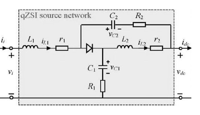
Figure 1. qZSI source network has two inductors and capacitors to handle energy storage during the shoot-through state. Image used courtesy of Bob Odhiambo
During the shoot-through state, current circulation occurs within the quasi-z network after simultaneously activating both switches in one inverter leg. In this mode, the current does not flow into the inverter bridge. To better understand the voltage boost mechanism, the duty cycle (Ts) of the shoot-through state is considered and used to evaluate the inverter's boost factor (B). As current flows through the two inductors in the network, energy is stored, boosting the voltage across the capacitors, which increases the inverter’s overall DC link voltage.
\[B=\frac{1}{1-2T_{s}}\]
By boosting the voltage before inversion, higher AC output voltage can be achieved even in cases where there is a low DC input voltage. Assuming a qZSI has a duty cycle of 0.25, the boost factor equals 2, as shown below, meaning the output voltage doubles the input voltage.
\[B=\frac{1}{1-2\times0.25}=\frac{1}{1-0.5}=2\]
This means that as the duty cycle increases, the boost factor increases, as shown in Figure 2. For instance, the boost factor at a duty cycle of 0.1 is about 1.11 while a duty cycle of 0.4 has a boost factor of approximately 1.67.
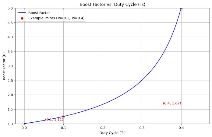
Figure 2. Relationship between quasi-z-source inverter's duty cycle and its boost factor. Image used courtesy of Bob Odhiambo
Once the voltage is boosted in the shoot-through state, the inversion process of the DC to AC in the non-shoot-through state can be done where the inverter bridge is supplied with the stored energy from the charged capacitors. A standard pulse width modulation technique (PWM) can convert the DC voltage to AC voltage output in a single stage. The modulated AC output voltage (Vac) of the qZSI inverter can be approximated by considering the modulation index M, expressed as shown below (Vdc), which is the DC input voltage.
\[V_{ac}=B\times V_{dc}\times M\]
Pulse Width Modulation for qZSI Control
Three PWM techniques for qZSI control include simple boost control (SBC), maximum boost control (MBC), and constant boost control (CBC), which influence the stability, efficiency, and switching losses in the inverter. These PWM methods have their share of strengths and limitations in qZSI control. SBC involves the insertion of a shoot-through state into the modulation signal when the carrier signal is below the predefined reference. This modulation method modifies the shoot-through duty cycle to achieve the desired voltage boost. Regarding efficiency, SBC has a lower efficiency at high boost factors than CBC and MBC due to high switching losses resulting from continuous switching. The high switching frequency in this PWM control method may also introduce harmonic distortion in the qZSI.
MBC PWM technique works by optimizing the usage of DC voltage by adjusting the shoot-through state to coincide with the reference signal’s zero crossing points. This minimizes loss during switching by applying shoot-through in periods with the lowest voltage across the impedance network. Unlike SBC, MCB is more efficient as it avoids continuous switching during peak voltage conditions. CBC balances efficiency and voltage boost by making dynamic adjustments to the shoot-through duty cycle regarding load conditions and output needs. This allows for consistency regardless of the varying load and reduces the overall stress on the inverter's components.
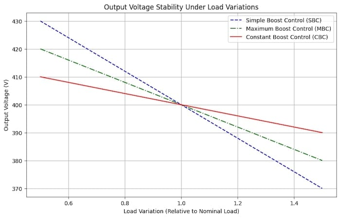
Figure 3. The output voltage stability in varying loads for the three PWM techniques in which CBC features a more stable output voltage. Image used courtesy of Bob Odhiambo
Renewable Energy Integration Applications
Due to qZSI's ability to offer power conversion even in power fluctuations, it can be easily integrated into the photovoltaic (PV) system to handle the issues of low irradiance or partial shading. This inverter topology also offers voltage stability from the PV arrays, and with dynamic adjustments of voltage and current, maximum power point tracking (MPPT) can be simplified.
QZSI inverter topology also works well in wind or hybrid systems combining wind and solar. The varying output voltage from wind turbines can be easily stabilized with the buck-boost capabilities of this inverter topology. With the growing adoption of green energy, the need for power conversion systems that offer efficiency and reliability increases. Power engineers can draw insights into which topology works best for a more stable power output.