Facebook
 Google
 GitHub
 Linkedin
Eggtronic Unveils a New Demo Board Aimed at Streamlining the Design of Compact, Efficient 35 W Adapters and Chargers
The new board employs the company’s proprietary EcoVoltas QuarEgg+ technology, and can be specified with either a GaN or Silicon FET.
Eggtronic’s QuarEgg+ employs a zero-voltage switching architecture with which to build efficient AC/DC flyback converters. Its design has been optimized to provide greater efficiency than either quasi-resonant flyback or active clamp converters, while still offering the lower costs often associated with the former.

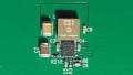
The board. Image used courtesy of Eggtronic
EcoVoltas, the architecture on which QuarEgg+ is built, was developed to aid designers in reducing cost, size, and weight while achieving sustainability goals. Though the technology, first introduced last December, remains strictly proprietary, Eggtronic has released several details. The architecture involves the use of zero-voltage switching under all load conditions, and obviates the need for a costly high-voltage, high-side clamping FET.

A QuarEgg+ schematic. Image used courtesy of Eggtronic
QuarEgg+ itself is built around an EPIC101AxQExx family secondary side controller, which implements primary side driving and synchronous rectification, and can provide USB-C Power Delivery Revision 3.1 capabilities. While the schematic defines a USB-C device, for added flexibility the development board is also suitable for fixed power output applications.
The Choice of GaN or Silicon FETS
Gallium nitride (GaN) semiconductors offer significant advantages over silicon (Si) devices. Notably, they can turn on and off faster, which makes for DC pulses with smaller time delays. This, in turn, allows for physically smaller filtering components. The end result is OEM products that are smaller, lighter, and more power efficient.
GaN has played a key role in fueling the new wave of wide bandgap semiconductors, as has silicon carbide (SiC). Still, conventional silicon is cheaper, and so Eggtronic has offered both options in its new board. Engineers seeking top performance will benefit from the advanced capabilities of GaN FETs, while those looking for cost-effective solutions can employ the silicon version.
Specifications
Eggtronic's demo board measures at just 38.3 x 38.3 x 18.6 mm. This is in line with the company’s converters; it claims its silicon converter is twice as small and suffers five times fewer losses than others on the market, while its GaN offering suffers two times fewer and is 30% smaller.
The board can operate from inputs ranging from 90 to 264 VAC. Output options include:
- 5 V at 3 A
- 9 V at 3 A
- 12 V at 2.9 A
- 15 V at 2.3 A
- 20 V at 1.75 A
The design sports a flat efficiency curve, peaking at 94%. Vital to so many modern applications, no-load power consumption (colloquially described as “vampire power”) is specced at less than 18 mW.
Other Members of the EcoVoltas Family
As it’s based on QuarEgg+ technology, the board is best suited for design in low-power applications, generally 75 W and less. For higher-power applications, the EcoVoltas family includes SmartEgg for use between 75 and 1000 W, and ClassEgg, for uses demanding power in excess of 1000 W.