Facebook
 Google
 GitHub
 Linkedin
Applied Materials Introduces Silicon Solar SunFab Thin Film Line
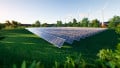
Applied Materials, Inc. introduced its Applied SunFab™ Thin Film Line, which is claimed to be the world’s first and only integrated production line for manufacturing thin film silicon solar modules using 5.7 square meter (m2) glass panels. These ultra-large substrates, sized at 2.2m x 2.6m, are said to be four times bigger than today’s largest thin film solar production panels. The Applied SunFab Line is said to define a new standard for the industry that can be replicated by customers to rapidly establish solar panel manufacturing capacity and achieve the lowest production cost per watt to drive down the cost of solar electricity.
The Applied SunFab Thin Film Line can be configured with single or tandem junction technology and is designed to produce enough solar modules in a year to generate up to 75MW of electrical power. Using 5.7m² panels, the SunFab Line can reduce the cost of utility-scale and building-integrated photovoltaic (BIPV) system installations by more than 20%. The company claims that it has already received multiple contracts for its SunFab Thin Film Line from customers in Europe and Asia.
"We’ve built on our years of experience in semiconductor and flat panel display manufacturing to create the solar industry’s first standardized thin film solution for making solar modules using cost-efficient, ultra-large glass panels," said Dr. Mark Pinto, Senior Vice President, Chief Technology Officer and General Manager of Applied’s Energy and Environmental Solutions group. "With this state-of-the-art thin film production line and Applied’s global service capabilities, we are well-positioned to accelerate the growth of the solar market by providing an unprecedented ’cost per watt’ through standardization, scale and efficiency."
According to the company, the SunFab Line’s design can deliver leading-edge solar manufacturing capability, using what is said to be the most advanced engineering, process equipment, diagnostics, automation and emissions abatement systems. Applied adapted its CVD and PVD process systems to build the most critical layers of the module, including its PECVD system that processes 5.7m² glass substrates for the flat panel display industry.