Facebook
 Google
 GitHub
 Linkedin
Alpha and Omega Unveils a Wireless Charging Solution for 50 Watt Applications
The AOZ32034AQV from Alpha and Omega Semiconductor is a highly integrated half-bridge power stage that lowers both the BOM and design time for wireless charging transmitters.
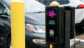
Wireless charging is becoming ever more popular, as consumers seek to avoid the inconvenience of endlessly connecting and disconnecting power cables, in addition to the cost of buying and replacing them. That in mind, Alpha and Omega Semiconductor's (AOS) new AOZ32034AQV coil driver is designed for a range of popular devices, from vacuum cleaners to drones and cordless power tools.
The AOZ32034AQV hosts many of the necessary components itself, including both high-side and low-side MOSFETs within its tiny 4 x 4 mm QFN package. In so doing, it simplifies the design of wireless chargers based on full-bridge topologies.
The Basics of Wireless Charging
Before diving further into the AOZ32034AQV’s specs, let’s quickly refresh how wireless charging works in the first place.
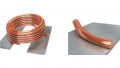
The charge generated in wireless charging is created via radio waves at frequencies harmless to humans. On the receiving end, the charging device has its own antenna system to intercept the power, and circuitry to convert it into useful DC.
The AOZ32034AQV, in Detail
The AOZ32034AQV is a 50 W version of the 30 W AOZ32033AQI, which AOS released last October. Like its predecessor, the new AOZ32034AQV employs a full-bridge topology with a resonant tank circuit for highly efficient power conversion.
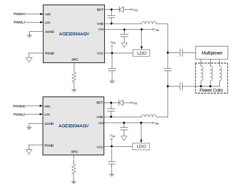
Two half-bridge AOZ32034AQVs used to implement a full-bridge wireless charging transmitter with a resonant tank circuit. Image used courtesy of AOS
The AOZ32034AQV can operate over an input range of 4 V to 28 V across a power range of 15 to 50 W. It employs n-channel FETS for both the high side and the low side, enabling better performance than would be possible with high-side p-channel devices. MOSFET RDS(ON) for the new device is 7.5 mΩ, an improvement over its predecessor’s 11.0 mΩ.
The device’s thermally-enhanced QFN package serves to direct heat away from the AOZ32034AQV itself, easing its transfer to the PCB for dissipation. This reduces the need for heat sinks and like devices, and allows the unit to safely handle more power.
Shoot-Through Protection
There are two inputs, HIN and LIN, that control the high-side and low-side MOSFETS, respectively.

A functional block schematic for the AOZ32034AQV. Image used courtesy of AOS
The device is designed so that HIN and LIN can not both fire their MOSFETs at the same time. There is also protection against under-voltage and over-temperature; If over-temperature of 140 ℃ is detected, the unit turns off until VCC, the supply voltage for internal analog functions, is reset.
The Compromise Between EMI and Efficiency
The transmitters in these systems beget some amount of unwanted emission, which often takes the form of harmful electromagnetic interference (EMI). EMI can be lessened by adjusting the slew rate of the MOSFET-controlling driver, and the AOZ32034AQV contains the necessary circuitry to do so.
In some applications, EMI control is vital. In others, efficiency takes precedent. Thus, an adjustable slew rate allows designers to optimize their systems.
Physical Considerations
- The AOZ32034AQV operates over an ambient temperature range of -40 °C to +125 °C
- The unit is available in a 4 × 4 mm QFN-23L package
Environmental Compliance
- The unit is RoHS Pb-compliant