Facebook
 Google
 GitHub
 Linkedin
2D Barcodes Help Track GaN Production Chip Origins
Cambridge GaN Devices has released the first-ever GaN devices with individual 2D barcoding to assist with die-level data collection for process, reliability, and quality improvement.
Cambridge, U.K. start-up Cambridge GaN Devices (CGD) has released the first-ever production of gallium nitride (GaN) power chips with 2D barcoding incorporated in the top marking to allow ICs to be uniquely identified by a commercial code reader.

2D barcoding on a packaged GaN device. Image used courtesy of CGD
Barcode identification will allow for the easy and rapid tracking of each chip (die) within CGD’s packaged power devices beyond standard wafer and assembly lot information, including the specific location of the wafer and where the die originated.
Die-level tracking will assist CGD with collecting precision quality and performance data to improve process ruggedness, reliability, and production yields.
Better Data to Improve Reliability and Yields
While CGD believes they already have sufficient performance data to demonstrate the ruggedness and reliability of their ICeGaN HEMT (high electron mobility transistor) technology, according to CEO Giorgia Longobardi, GaN processes are still relatively new compared with silicon, so more proactive steps are required to demonstrate their reliability.
With easy-to-read barcoding on the top of each production IC, quality information can quickly be communicated back to manufacturing and production teams to implement process improvements that directly impact device quality, reliability, and production yields.
These initiatives are particularly important as GaN devices scale to higher production levels, where the scope of any reliability or yield issue will be much greater, impacting device costs, availability, and, potentially, customer applications in the field.

Semiconductor wafer manufacturing. Image used courtesy of Emerson
Importance of Wafer Location
Zahid Ansari, CGD’s VP of Operations, stated it is well known that die harvested from the edges of a semiconductor wafer tend to have lower production yields due to higher defect densities. This means that comparatively fewer die from these areas can successfully pass through the testing process and make it to final inventory as production units.

Semiconductor wafer mapping. Image used courtesy of Onto Innovation
As production yields drop, costs increase, thus hurting margins for the manufacturer and raising costs for end customers who inevitably bear some of the burden through cost pass-throughs.
By tracking production yields and relaying individual die quality information in near real-time to manufacturing teams, adjustments can quickly address problem areas and recover yields.
Testing Semiconductors
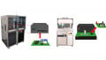
Designing a semiconductor chip starts with the process selection. The semiconductor wafer is developed through a step-by-step process that forms the individual devices, or circuits, within the wafer.
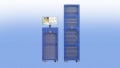
As a first test, each die (IC) within the wafer is tested with a probe system to identify faulty die resulting from wafer defects. The wafer is then “sliced” into individual die, and the “known good die” are passed along for either package or wafer-level assembly.
After final assembly, the part is passed through a final automated test program to verify it meets performance specifications before being released to inventory for eventual commercial sale.
_production_testing.jpg)
Integrated circuit (IC) production testing. Image used courtesy of National Instruments
Reducing the number of bad die and identifying them early in the manufacturing process improve production yields and help to maintain costs. For newer products and technologies, like GaN, optimizing device yields can take time and many production iterations.
Field Reliability
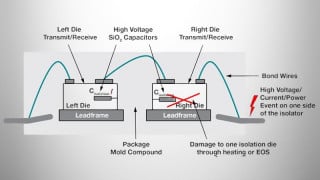
Despite rigorous testing at the wafer level and final assembly, some flawed units will escape detection and find their way into customer applications. These “field failures” are typically returned to the factory for decapsulation and imaging by the QA (quality assurance) team to determine the cause of the failure.
Field failures are often the result of improper use of the device. One example is engineering overstress (EOS), where the specified limits of the device, such as withstand voltage and short-circuit current, are exceeded. For other cases, identifying the origins of a die via an easily readable barcode can help the manufacturer develop a clearer picture of potential process issues that may be impacting the field reliability of their devices.

IC decapsulation and imaging. Image used courtesy of Silconic
Integrated Circuit Enhancement Mode GaN (ICeGaN)
GaN-based circuits offer high power densities with fast switching speeds and good efficiency. However, GaN devices can be difficult to work with, requiring specialized drive circuits that add to design complexity, component count, and cost.

Switching supply schematic with ICeGaN device. Image used courtesy of CGD
Integrated Circuit Enhancement Mode GaN (ICeGaN) is a technology commercialized by CGD that allows a GaN transistor to be operated like a silicon MOSFET device using standard gate drive circuits.
With ICeGaN, negative voltages are not required for device shutdown, eliminating the need for costly and complex conversion and clamping circuits that standard silicon devices do not require.