Facebook
 Google
 GitHub
 Linkedin
Powering IGBT Drivers with TI039s FlyBuck Converter
This article offers methods of using Fly-Buck converter as a cost-effective and simpler solution to power IGBT driver in the AC motor drives and inverters.
Insulated-gate bipolar transistor (IGBT) are widely used as the main power-carrying device in high-voltage and high-current systems. These types of systems include variable-frequency AC motor drives (VFD), industrial uninterruptible power supply (UPS) systems, and solar inverters.
In these applications, IGBTs are often configured in a bridge connection, and switch on and off alternately to drive high-current pulses into the motor coils or transformer windings. The reliability and robustness of an IGBT-based system is critical as it handles power from kilowatt to megawatt level.
Compared to the whole system, the IGBT gate driver only consumes “pea-sized” power, or just a few watts. However, it is the driver that helps to ensure that the IGBT has reliable switching. The high-voltage and current swing in the IGBT switching presents great challenges to the driver design, and usually requires a dedicated bias power supply.
IGBT Gate Driver Supply Requirements
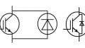
Multiple isolated positive and negative voltage rails are often required to power the IGBT drivers in a system. The positive voltage is for turning on the IGBT. It should hold a steady voltage level as it affects the turn-on speed. The negative bias is required for a reliable IGBT turn-off. During the switching transient, the high dv/dt swing could induce the gate voltage to jump high momentarily. If the gate driver bias is not pulled at a low enough negative potential, it could lead to the IGBT falsely turning on and increase the risk of high-current shoot-through. Isolation is another requirement for the driver bias supply. In a multi-phase IGBT system, the high-side driver needs an isolated bias for each phase. Sometimes the preference is to have isolation for low-side IGBTs as well to avoid any ground noise interference. Figure 1 shows the gate drivers for two IGBTs in a half-bridge configuration, which needs two pair of bipolar voltage rails.

Figure 1: Gate drivers with bipolar bias for two IGBTs
Push-pull, flyback, and forward converters have been the common choices of isolated power supply topologies for IGBT driver bias. The bias outputs are obtained through an open-loop switching or auxiliary transformer winding feedback control. The open-loop operation gives poor line and load regulation. It relies on a stable input DC source and post-stage low dropout (LDO) regulators to produce stable bias rails.
On the other hand, the auxiliary winding feedback method adds more required windings and pins to the transformer. The cross-regulation between outputs is not optimal. However, the Fly-Buck converter can readily take on the task. The topology uses a transformer in a buck converter instead of an inductor to generate isolated outputs (Figure 2). It controls the secondary side outputs by regulating the primary side output similar to a normal buck. The Fly-Buck uses the primary output to clamp the secondary outputs through coupled windings. This primary-side regulation makes it easy to obtain well-controlled isolated voltages without needing an auxiliary winding or optocoupler feedback. In general, the topology has balanced cross-regulation performance, and the switching operation is less noisy.

Figure 2: Fly-Buck converter topology
Fly-Buck Driver Bias Considerations
When using a Fly-Buck to power IGBT drivers, the optimal configuration of the supply for the system should be evaluated. Depending on the application case, there are several ways to configure the outputs as one Fly-Buck can provide the bipolar voltages for one or multiple IGBT drivers. For a single IGBT, the driver bias needs one pair of positive and negative outputs. For two IGBTs in a half bridge, the bias supply should have four outputs. For a typical three-phase AC motor, the six IGBTs require at least eight bias outputs for the gate drivers, as the three bottom side IGBTs share the common ground and can use the same bias rails for the drivers.
From a cost perspective, a centralized power supply that covers the whole system’s driver bias needs is more beneficial than the discrete solution. However, having separate driver supplies gives improved performance in terms of stable regulation and higher power capability. Also, it may be impractical to have a centralized solution as the safety spacing between isolated outputs from the insulation requirement may make the transformer design unfeasible to fit all the windings in one package. To obtain the positive and negative outputs, besides using two transformer windings, these outputs can also come from a single winding with the voltage-split circuit (Figure 3). The two-winding solution has a better regulation and efficiency overall, but the voltage-split method halves the number of secondary windings, making it more suitable for a multiple-driver Fly-Buck supply.


Figure 3: Generating the bipolar bias using (a) dual windings; and (b) one winding and a voltage split circuit.
The gate voltage bias levels vary, based on the IGBT selection and system operating conditions. Typically, the positive voltage is set at 15V to 18V range, whilst the negative voltage level is more flexible; it can be symmetrical to the positive rail, or have a lesser voltage of –5V to –10V. The negative rail is often deemed less critical than the positive one, and allows a higher variation tolerance. In an actual design case, the bias levels may need to be optimized according to the system test and performance. A Fly-Buck converter has the flexibility to accommodate changes by adjusting the primary buck output voltage after the transformer’s turns ratio is fixed.
The power required to drive an IGBT is also an important specification and can be estimated by:
`P_g=ΔV_g*Q_g*F_(sw)`
where ΔVg is the positive to negative gate voltage swing, Qg is the total IGBT gate charge at the given bias level, and Fsw is the IGBT switching frequency.
The gate driving power, plus the driver IC and circuit’s own consumed power, is the total required power for the driver bias supply. This is usually a few watts, and the bias supply current is less than 1A. However, the gate driver current can have a much higher spike of 5A-10A or even above at the switching instants. The bias supply needs to have sufficient output capacitance to minimize the output ripple.
Design and Examples
After determining the bias power configuration, the Fly-Buck design process is similar for both multiple-driver and single-driver solutions. The first step is to set the primary output voltage. Since the Fly-Buck primary side is a buck topology, the primary output cannot be higher than the topology that uses the off time to transfer energy. A duty cycle too high leads to high secondary peak current and poor regulation.
The input voltage for the driver bias is usually taken from the system’s auxiliary power rail at 24V or 12V. For a 12V-based input voltage, it is difficult to find an ideal primary voltage point. If following the 50 percent duty cycle rule, the primary voltage should be set at a low level so that the transformer windings need a high step-up ratio to generate the isolated bias, which can damage the regulation.
To improve the low input performance of the Fly-Buck, the primary side can be set as an inverting buck topology. The inverting buck (or buck boost) generates a negative output, and the buck converter IC uses the negative voltage as its ground reference. It lowers the duty cycle and effectively extends the Fly-Buck’s operation range in low-input voltage conditions.
The transformer turns ratio can be determined after setting the primary output. The secondary-to-primary winding turns ratio is roughly equal to the secondary-to-primary voltage ratio. A more realistic estimate is to include the rectifier diode forward voltage and the winding resistance voltage drop. The average current in the primary winding can be calculated as the sum of the secondary output current reflected to the primary:
`I_(pri)=K*\sum_{i} N_i*I_(sec(i))`
where Ni is the secondary-to-primary turns ratio for the ith winding, and the coefficient K is equal to 1 for normal Fly-Buck, and 1/(1-D) for inverting buck configuration.
The current level is higher when using the inverting buck. The current ripple should be less than 60 percent of the average, and the minimum desired inductance of the transformer primary side can be calculated. The peak current needs to be checked so that it does not exceed the current limit of the Fly-Buck converter integrated circuit (IC).
To demonstrate the design, I created two reference board examples. One is an eight-output Fly-Buck bias for six IGBT drivers in a three-phase motor (Figure 4), and the other is a two-output Fly-Buck for a single driver (Figure 5). In both design examples, I used the Texas Instruments’ LM5160 buck converter for the Fly-Buck regulator. This device is a constant on-time (COT) synchronous buck converter. It can operate in a wide input range of 4.5V to 65V, and has 1.5A current capability with integrated FETs and can be used for Fly-Buck applications.

Figure 4: Eight-output Fly-Buck supply powering six IGBT drivers in a three-phase motor

Figure 5: Two-output Fly-Buck power supply powering a single IGBT driver
The eight-output reference design is for the 24V-based input voltage, and the input is allowed to vary from 20V to 30V. The power supply provides +15V and –8V bias rails with 100 mA current capability for each IGBT driver. The reference board is shown in Figure 6 uses one transformer with four secondary windings, where the +15V and –8V rails are produced by a voltage-split circuit. The primary voltage is set at 10.5V, and the turns ratio is set at 2.3:1 to get a total 23V from one secondary winding.
Three pairs of the isolated +15V, –8V outputs with 100 mA current is for the three top IGBTs. The other bipolar outputs have 300 mA output current for the three bottom IGBT drivers combined. So the average current on the primary side is at about 1.4A, which is enough margin from the 2.1A peak current limit of the LM5160 Fly-Buck IC. The +15V output with the Zener clamp has stable voltage, within five percent regulation over line or load variation. Note that the –8V outputs can endure all variations from the single-winding output, which can hold below –6.5V at full load. The peak power efficiency is about 82 percent. The design was validated with 1200V IGBTs and 6A gate driver in a three-phase system.

Figure 6: Reference board of the eight-output Fly-Buck bias design
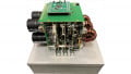
The two-output design is for the 12V-based system. It has an input range of 8V-20V, and generates +15V and –9V outputs at 200 mA max current. It uses the inverting buck setting in order to operate at the low-input voltage level, and has separate windings for the bipolar outputs. The primary output is set at –15.3V, and the turns ratio is 1:0.6:1. It achieves five percent regulation for both outputs and has better efficiency with 87 percent peak. This reference board also features a module-like design, with a compact size of 28x18-mm and a DIP 22-pin package footprint (Figure 7).

Figure 7: Reference board of the two-output Fly-Buck bias design
The tradeoff between the two designs is clear. The centralized design with one converter IC and one transformer is more cost-effective for a three-phase motor system, but the single-driver design doubles the bias power capability and has better performance. They suit different applications depending on the system needs.
A Summary of the Fly-Buck's Features
The Fly-Buck converter brings a cost-effective and simple-to-use power solution to power the IGBT driver in the AC motor drives and inverters. The Fly-Buck features the primary side regulation. It also can provide good cross-regulation, wide-input operation, and low-noise interference, so it can meet the stringent requirements posted in these application spaces. For different IGBT-based systems, the converter can be configured to power one or more IGBT drivers giving your design greater flexibility.
About the Author
Xiang Fang works as the System Applications Engineer at Texas Instruments since April 2012. He specializes in switched-mode power supply (SMPS), DC/DC converter, resonant converter and related power electronic products design, simulation, analysis and testing. Xiang earned his Bachelor's Degree in Electrical Engineerig at Tsinghua University. He also holds a Ph.D. in Power Electronics at the University of Central Florida.
References
- Fang, X.; Liu, W.; Chadaga, A., “Fly-Buck adds well-regulated isolated outputs to a buck without optocouplers,” EDN,06 Apr. 2014
- http://edn.com/design/power-management/4429791/Product-How-to--Fly-Buck-...
- Fang, X.; Meng, Y., “Isolated Bias Power Supply for IGBT Gate Drives Using the Fly-Buck Converter,” Applied Power Electronics Conference and Exposition (APEC), 2015 IEEE, pp.2373,2379, 15-19 March 2015
- LM5160 datasheet: www.ti.com/product/lm5160
- TI Reference Design: Wide-Input Isolated IGBT Gate-Drive Fly-Buck Power Supply for Three-Phase Inverters: http://www.ti.com/tool/TIDA-00199
- TI Reference Design: Dual Isolated Outputs Fly-Buck Power Module Design for Single IGBT Driver Bias: http://www.ti.com/tool/PMP10654