 Facebook
 Google
 GitHub
 Linkedin
Why Source-Down, Double-Sided Cooling MOSFET Packaging Is Advancing AI Server Power Density
As the evolution toward higher power density in AI data centers continues, it demands innovation in MOSFET packaging to overcome thermal constraints. By transitioning to double-sided cooling and advanced copper interconnects, infrastructure designers can bypass traditional thermal bottlenecks and maximize power efficiency in next-generation systems.
This article is published by EEPower as part of an exclusive digital content partnership with Bodo’s Power Systems.
Meeting the Thermal Challenge of Next-Generation AI Infrastructure
The rapid expansion of artificial intelligence (AI) computing has dramatically increased power demands within modern data centers. AI accelerators and high-performance GPUs require sophisticated power delivery architectures capable of handling hundreds of amperes while maintaining exceptional efficiency and reliability. As a result, thermal management has become one of the most critical design considerations for engineers developing high-current DCDC converters such as the intermediate bus converters (IBCs).
As designers seek to deliver more power within increasingly compact footprints, thermal limitations often become the primary constraint rather than silicon capability. Efficient heat removal allows systems to operate at higher current densities while minimizing board area.
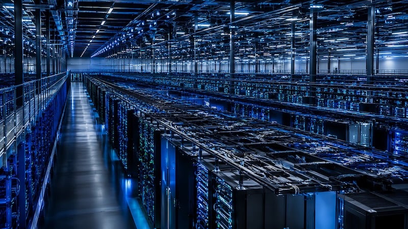
Figure 1. High-density server environment. Image used courtesy of Bodo’s Power Systems [PDF] and Adobe Stock (licensed).
While semiconductor process technology continues to improve MOSFET electrical performance, packaging innovation is emerging as an equally important factor in achieving higher power density. One notable advancement is the adoption of source-down, double-sided cooling packaging, which addresses thermal bottlenecks and simplifies the component layout on the printed circuit board (PCB).
One of the primary thermal constraints in AI servers may no longer be the silicon MOSFET technology, but rather the ability to remove the heat generated during the power conversion stages.
Traditional DFN power packages primarily dissipate heat through a single thermal path. As current levels increase, this single-sided approach can create localized hot spots, limiting system performance and reducing design margins.
A source-down package with double-sided cooling introduces an alternative architecture by enabling heat removal through both the top and bottom of the device. This creates multiple thermal pathways to attached heat sinks or cooling structures, reducing thermal resistance and improving overall heat extraction. The source down allows thermal vias to improve heat removal.
For AI server applications operating under sustained heavy loads, distributing heat through two interfaces rather than one can significantly reduce junction temperatures and improve long-term reliability.
Double-Side Cooling Technology
Top-side cooling technology with large copper clips significantly enhances both electrical and thermal package reliability. This clip-bonding technology expands the "surface contacts," effectively establishing the solid copper clip as a high-performance internal heat spreader.
By exposing a large, direct metallic contact on the upper surface of the package, this architecture achieves an exceptionally low junction-to-case thermal resistance (Rthjc-top).
Under the Source-Down architecture, the silicon die is inverted to place the source potential in direct contact with the system ground planes, which, combined with a top-side drain clip, ensures that heat is vertically channeled toward external cooling interfaces rather than remaining trapped within the thermally insulating mold compound.
By utilizing both surfaces of the package for heat dissipation, double-sided cooling allows two thermal paths between the silicon die and the cooling solution. Improved thermal performance enables MOSFETs to sustain higher power levels without exceeding safe operating temperatures.
Lower operating temperatures reduce thermal stress on semiconductor devices and surrounding components. This contributes to improved long-term reliability, particularly in continuously operating AI servers and cloud infrastructure.
The source-down package offers benefits beyond thermal performance. The source connection directly connects to the PCB via a larger contact area, minimizing electrical resistance while improving mechanical robustness. In addition, a center-gate layout simplifies PCB routing, allowing designers to shorten gate driver connections and optimize switching performance.
These packaging characteristics help engineers reduce layout complexity while improving manufacturability and electrical efficiency.
25V, 40V and 80V MOSFETs in State-of-the-Art Package
48V Intermediate Bus Converters represent a critical stage in AI server power distribution, converting bus voltages into lower rails that feed multiphase regulators powering GPUs and AI processors. These converters must deliver extremely high currents with minimal losses and excellent thermal performance.
Employing MOSFETs with source-down and double-sided cooling technology is well suited for these applications because it combines low power losses with efficient heat removal. The package supports operation under demanding thermal conditions while enabling designers to increase power density without sacrificing reliability.
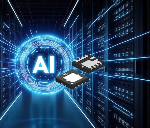
Figure 2. 25V and 80V MOSFETs in State-of-the-Art Packaging. Image used courtesy of Bodo’s Power Systems [PDF] and Alpha and Omega Semiconductor.
This article highlights Source-Down packaging technology, such as the Alpha and Omega Semiconductor (AOS) AONC40202 25V, AONC68410 40V, AONC68816, and AONC68817 80V MOSFETs, in which the source pad can connect to the ground plane. AOS 25V, 40V, and 80V technologies and Source-Down package configuration will minimize switching noise and enable two paths for heat flow that prevent energy from being trapped within the package, which degrades performance.
The implementation of high-performance MOSFETs such as AONC40202, AONC68410, AONC68816, and AONC68817 offers higher efficiency and better thermal dissipation. This allows the components to operate at lower junction temperatures (Tj). This translates into improved power usage effectiveness (PUE) for the data center, as higher component efficiency reduces energy demand from external cooling systems.
Conclusion
As AI workloads continue to scale, advances in semiconductor packaging are becoming as important as improvements in device silicon. Source-down and double-sided cooling MOSFETs provide a compelling solution for overcoming thermal constraints in highcurrent power conversion by enabling superior heat dissipation, increased power density, and simplified PCB design.
For engineers developing AI servers and data center power systems, adopting double-sided cooling package technology offers a practical path toward higher efficiency, greater reliability, and the performance required by tomorrow’s most demanding compute platforms.
This article originally appeared in Bodo’s Power Systems [PDF] magazine.