Facebook
 Google
 GitHub
 Linkedin
The Circuit Description and Functionality of a Two Terminal Bipolar Power Supply
This article demonstrates a simple 2-quadrant voltage source circuit using the LTC8714.
A 2-quadrant power supply — one that provides a positive or negative voltage to the same output terminals — can easily be produced using the LT8714 4-quadrant controller. The 2-quadrant supply shown here can be used in a variety of applications ranging from window tinting — where changing polarity changes the alignment of crystal molecules — to test and measurement equipment.
The LT8714 data sheet describes the operation of the 2-quadrant supply in the first quadrant (positive input, positive output) and in the third quadrant (positive input, negative output). Note that in both quadrants the power supply is sourcing current, thus producing a power source, not a power sink. The second quadrant and fourth quadrant produce a power sink.
Circuit Description and Functionality
Figure 1 shows an electrical schematic of the LT8714 as a 2-quadrant power supply. The powertrain consists of NMOS QN1, 2, PMOS QP1, 2, inductors L1, L2, coupling capacitor CC, and input and output filters. Inductors L1 and L2 are two discreet, noncoupled inductors, an approach that can reduce the cost of the converter. Proper selection of active and passive components requires understanding the voltage stresses and current levels present in each quadrant. For this purpose, the functional topologies for the positive output are shown in Figure 2.

Figure 1: An electrical schematic of a power supply based on the LT8714 operating in two quadrants VIN 12 V, VO ±5 V at 6 A.
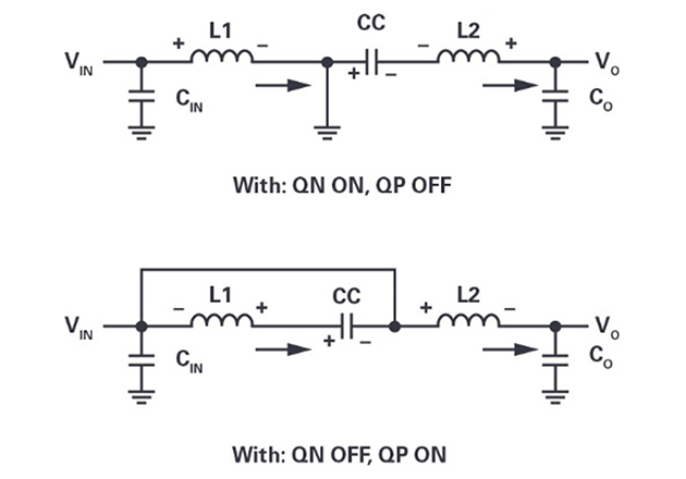
Figure 2: The topology of a 2-quadrant operation with a positive output.
When the volt-second balance is in a steady state, the duty cycle can be derived from the expression:
$$D = \frac{V_{IN} - V{O}}{2 \times V_{IN} - V_{O}}$$
To verify the design, demonstration circuit DC2240A was reworked to match the schematic shown in Figure 1. The input voltage is a nominal 12 V, with output voltages of ±5 V at a maximum current of 6 A for both. The measured efficiency for the design is shown in Figure 3. The positive output exceeds that of the negative output, which matches the results of theoretical calculations. The voltage stress and current on the components are much higher in the negative output configuration, increasing losses, and decreasing efficiency.
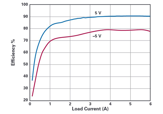
Figure 3: Converter efficiency curves with VIN 12 V, VOUT +5 V and –5 V, and a maximum IO of 6 A.
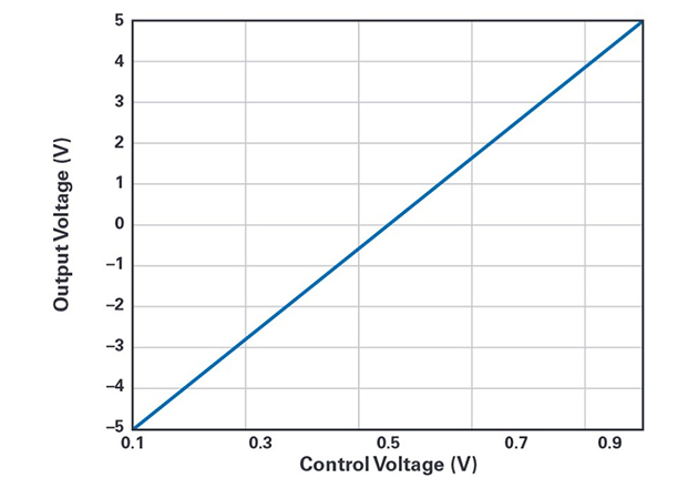
Figure 4: A graph of the output voltage, VOUT, as a function of control voltage, VCTRL. As VCTRL changes from 0.1 V to 1 V, the VOUT changes from –5 V to +5 V.
Figure 4 illustrates the excellent linearity of the output voltage vs. control voltage VCTRL. For this configuration, the circuit was loaded by a 1 Ω resistor, and the control voltage was varied from 0.1 V to 1 V. Using two LTspice® models, we were able to analyze the LT8714’s performance with a power good indication in the first model and using uncoupled inductors in the second model.
Conclusion
This article demonstrates a simple 2-quadrant voltage source circuit using the LTC8714. The design was tested and verified to have excellent linearity from the LTC8714 controller.
About the Author
Victor Khasiev is a senior applications engineer at ADI. Victor has extensive experience in power electronics both in ac-to-dc and dc-to-dc conversion. He holds two patents and has written multiple articles. His patents are about efficient power factor correction solutions and advanced gate drivers. Victor enjoys supporting ADI customers: answering questions about ADI products, the design, and verification of power supplies schematics, and the layout of the print circuit boards; troubleshooting; and participating in testing final systems.
This article originally appeared in the Bodo’s Power Systems magazine.